
Variable Delay (Programmable)
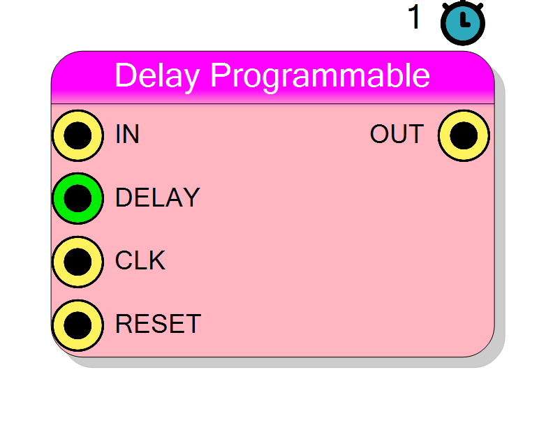
Programmable delay line with runtime-adjustable delay controlled by the DELAY input. Uses FPGA block RAM for efficient storage, allowing delays up to 65536 clock cycles. Provides 1 clock cycle inherent latency plus the programmed delay value. Ideal for applications requiring dynamic delay adjustments.
Introduction
This block implements a programmable digital delay line using FPGA block RAM, allowing the delay to be dynamically controlled at runtime via the DELAY input signal.
The delay is variable and runtime-programmable:
$$ \mathrm{OUT}(n) = \mathrm{IN}(n - D - 1), $$
where $D$ is the current value on the DELAY input (integer, range 0 to Max Delay Value). Note the inherent +1 cycle latency due to RAM read timing.
Pin Description
Bit Width bits (1-1024)
Data is written to the RAM circular buffer on every clock cycle.
Runtime-programmable delay value (integer). Range: 0 to Max Delay Value - 1
Actual output delay = DELAY + 1 clock cycles.
- DELAY=0 gives 1 cycle delay (minimum)
- DELAY=Max-1 gives Max cycle delay (maximum)
Changing DELAY takes effect on the next clock cycle.
Delayed output data signal.
Width: Bit Width bits (same as IN)
OUT(n) = IN(n - DELAY - 1)
Output is registered and valid on the rising edge of CLK.
Properties
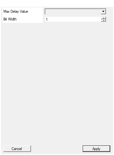
Set the amount of memory to reserve for this delay line
Maximum delay capacity (in clock cycles). Allowed values: 64, 128, 256, 512, 1024, 2048, 4096, 8192, 16384, 32756, 65536
This value determines the amount of block RAM allocated at compile time. The DELAY input must be in the range [0, MaxDelayValue-1].
Resource usage = MaxDelayValue × BusWidth bits of block RAM.
Default: 1024
Options: 64 128 256 512 1024 2048 4096 8192 16384 32756 65536
Set the size in bits of the signal to be delayed
Bit width of the input/output signals. Range: 1 – 1024 bits.
Total RAM usage = BusWidth × MaxDelayValue bits.
Each bit of width consumes additional block RAM proportionally.
Default: 1
Range: 1 – 1024
Functional description
The component uses a circular buffer implemented in block RAM. A write pointer continuously stores incoming data, while a read pointer (offset by the delay amount) retrieves delayed data. The DELAY input controls the offset between pointers.
Implementation details
- Storage: Uses FPGA block RAM (not registers)
- Minimum delay: 1 clock cycle (DELAY=0 gives OUT = IN delayed by 1 cycle)
- Maximum delay: Set by Max Delay Value property (up to 65536)
- Inherent latency: +1 clock cycle (RAM read latency)
- Total latency: DELAY + 1 clock cycles
Delay calculation
When DELAY input = $D$:
- Actual output delay = $D + 1$ clock cycles
- DELAY=0 → 1 cycle delay
- DELAY=5 → 6 cycle delay
- DELAY=1023 → 1024 cycle delay
When to use Variable Delay vs Fixed Delay
Use Variable Delay when:
- Delay needs to change dynamically at runtime
- Delay is large (typically > 16 clock cycles)
- Block RAM is available and preferred over flip-flops
Use Fixed Delay when:
- Delay is known at compile time and never changes
- Delay is small (< 16 cycles typically)
- You need exact latency matching without the +1 overhead
Timing
The component has variable latency based on the DELAY input:
| DELAY input | Latency (clock cycles) |
|---|---|
| 0 | 1 |
| 5 | 6 |
| M | M+1 |
where M is the Max Delay Value property.
Typical use cases
- Dynamic pipeline balancing: Adjusting delays to match processing paths
- Calibration systems: Fine-tuning timing during runtime calibration
- Buffer management: Creating adjustable data buffers
- Coincidence windows: Implementing variable-width coincidence logic
- Trigger delay: Programmable trigger alignment
Design considerations
Memory allocation
The Max Delay Value property reserves block RAM at compile time:
- Max Delay = 1024, Bit Width = 16: Uses 16 Kbits of block RAM
- Max Delay = 4096, Bit Width = 32: Uses 128 Kbits of block RAM
Delay limits
The DELAY input must satisfy: 0 ≤ DELAY ≤ Max Delay Value - 1
Exceeding this range will cause undefined behavior (may wrap around or corrupt data).
Minimum recommended delay
For very small delays (< 5 cycles), the legacy documentation recommends using the Fixed Delay block instead, as it’s more resource-efficient for short delays.
Waveform example
Example with Max Delay = 1024, Bit Width = 8, showing DELAY changing from 2 to 4.
Note: When DELAY=2, OUT lags IN by 3 cycles (2+1). When DELAY changes to 4, OUT lags by 5 cycles.