
Not Equal
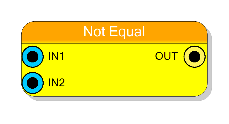
Compares two binary values and outputs a boolean result (1-bit) indicating whether they are NOT equal. Supports both signed and unsigned comparisons with configurable word sizes and optional output register for timing closure.
Introduction
This block performs an inequality comparison between two input values. The output is a single bit that indicates whether the inputs are different:
$$ \mathrm{OUT} = \begin{cases} 1 & \text{if } \mathrm{IN1} \neq \mathrm{IN2} \ 0 & \text{otherwise} \end{cases} $$
The component supports both signed and unsigned data types and offers an optional output register for improved timing performance.
Pin Description
Comparison result output.
- ‘1’ when IN1 does NOT equal IN2
- ‘0’ when IN1 equals IN2 Width: 1 bit
Properties
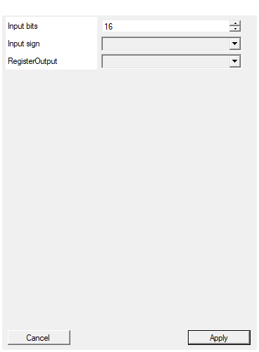
Set the number of bits of the input
Number of bits for each input value. Range: 2-2048 bits. Both inputs must have the same width.Default: 16
Range: 2 – 2048
Select the sign/unsign of the input
Selects the interpretation of input values: UNSIGNED (default) or SIGNED (two’s complement). For inequality comparison, this does not affect the result.Default: UNSIGNED
Options: UNSIGNED SIGNED
Enable one pipeline stage adding a register
Adds an output register stage. Disable (combinational, zero latency) or Enable (registered, 1 clock cycle latency) for timing closure.Default: Disable
Options: Disable Enable
Functional description
The Not Equal comparator checks whether two input values are different. The comparison is performed on the full bit-width of the inputs, and the result is a single boolean bit.
Comparison Operation
For both unsigned and signed numbers: $$ \mathrm{OUT} = (\mathrm{IN1} \neq \mathrm{IN2}) $$
Note: For inequality comparison, signed and unsigned interpretations produce the same result since we’re comparing bit patterns for any difference.
Truth Table
| IN1 | IN2 | OUT |
|---|---|---|
| 0 | 0 | 0 |
| 0 | 1 | 1 |
| 1 | 0 | 1 |
| 1 | 1 | 0 |
Latency and Timing
The component offers two latency modes:
| RegisterOutput | Latency (clock cycles) |
|---|---|
| Disable | 0 |
| Enable | 1 |
- Disable: Purely combinational logic, zero latency.
- Enable: One register stage added for timing closure in high-speed designs.
Typical use cases
- Change detection and monitoring
- Error detection in data streams
- Mismatch identification
- State machine transitions
- Data validation logic