
Float DIV TM
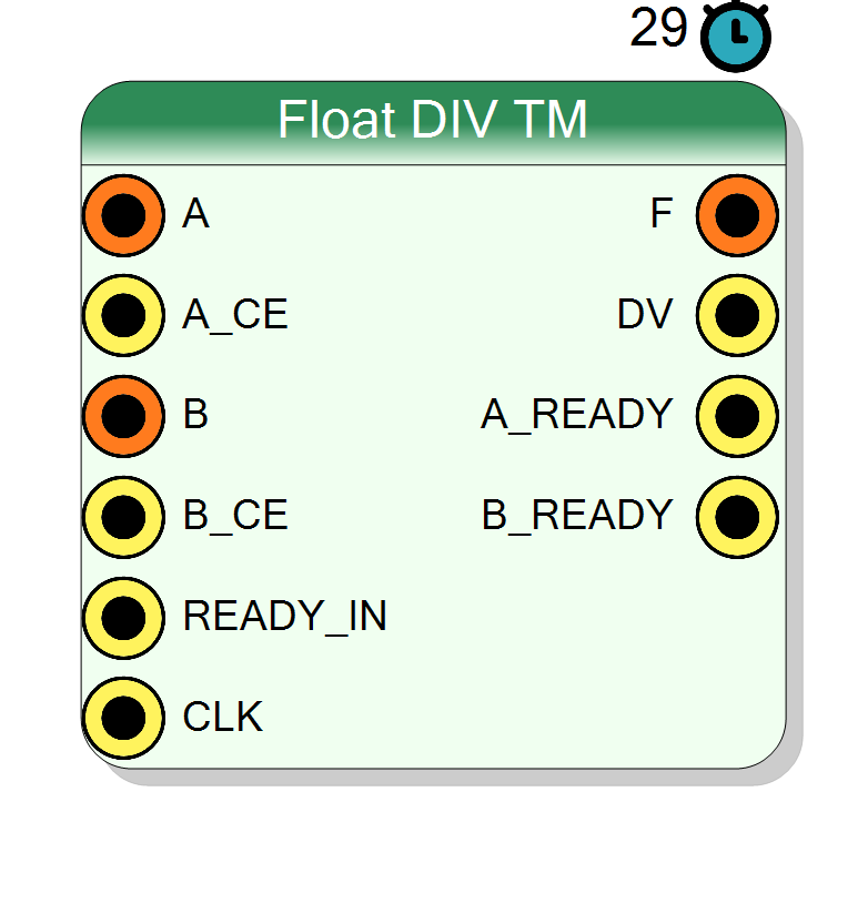
Time-multiplexed floating-point division operator based on Xilinx Floating Point IP. Supports single (32-bit) and double (64-bit) precision, configurable initiation interval, optional TM mode for divisor, and multiple TM phases (1-32) for high-throughput parallel computation in arithmetic processing pipelines.
Introduction
This block performs IEEE 754 floating-point division using the Xilinx Floating Point IP core. The component supports Time Multiplexing (TM): multiple parallel computation units (phases) share the same clock cycle, enabling high sample rates with predictable latency.
On every rising edge of CLK, if A_CE = 1, B_CE = 1, and READY_IN = 1, the operator performs
$$ \mathrm{F}(n) = \frac{\mathrm{A}(n)}{\mathrm{B}(n)}, $$
where all operands are IEEE 754 floating-point values.
Pin Description
(Exponent + Mantissa) × TMFactor
Floating-point divisor.
- If B is TM = YES: TM bus
- If B is TM = NO: Scalar (replicated)
Properties
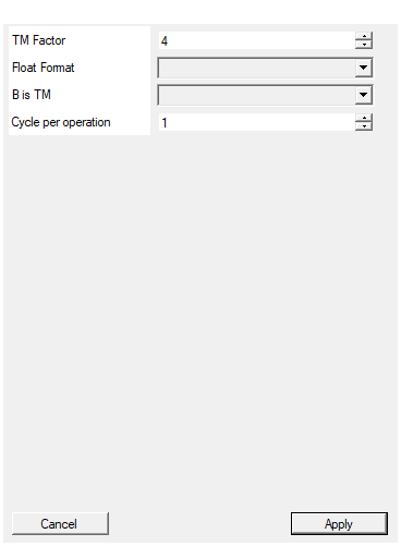
Time Multiplexing factor (number of phases)
Number of time-multiplexed phases (1 – 32).Default: 4
Range: 1 – 32
Select between single precision 32 bit and double precision 64 bit
Single→ 32-bitDouble→ 64-bit
Default: Single
Options: Single Double
Select if input B is Time Multiplexed or the same for all phases
YES→ B is TMNO→ B is scalar
Default: YES
Options: NO YES
Number of clock cycles to execute a division. Set to 1 to perform division in realtime. Higher number reduce the area usage of the block
Initiation Interval (Cycle per operation). Range: 1 – 26.
- 1 = Maximum throughput, maximum area
- Higher values reduce area usage
Default: 1
Range: 1 – 26
Functional description
The component wraps the Xilinx Floating Point IP (operation type: Divide)
and replicates it N times (where N = TM Factor) to support time-multiplexed
data streams.
Input modes
- Input A (dividend) is always TM
- Input B (divisor) can be either:
- TM mode (B is TM = YES): Each phase gets its slice
- Broadcast mode (B is TM = NO): Single value replicated to all phases
Output
- Output
F(quotient) is always TM
Mathematical background
IEEE 754 floating-point division with proper rounding:
$$ \frac{x}{y} = \text{round}\left(\frac{x}{y}\right) $$
Special cases:
- $\frac{x}{1} = x$
- $\frac{0}{x} = 0$ (for $x \neq 0$)
- $\frac{x}{0} = \infty$ (for $x \neq 0$)
- $\frac{0}{0} = \text{NaN}$
- $\frac{\infty}{\infty} = \text{NaN}$
Timing
The Xilinx Floating Point IP has a fixed latency of 29 clock cycles per phase:
| Property | Latency (cycles) |
|---|---|
| Division | 29 |
Initiation Interval (II)
The Cycle per operation property (II) controls the throughput/area trade-off:
- II = 1: New operation every cycle (maximum throughput, maximum area)
- II > 1: Fewer resources, reduced throughput
Range: 1 – 26 cycles.
Typical use cases
- Normalization
- Ratio calculations
- Reciprocal scaling
- Average computation
- Control algorithms