
G-PORT
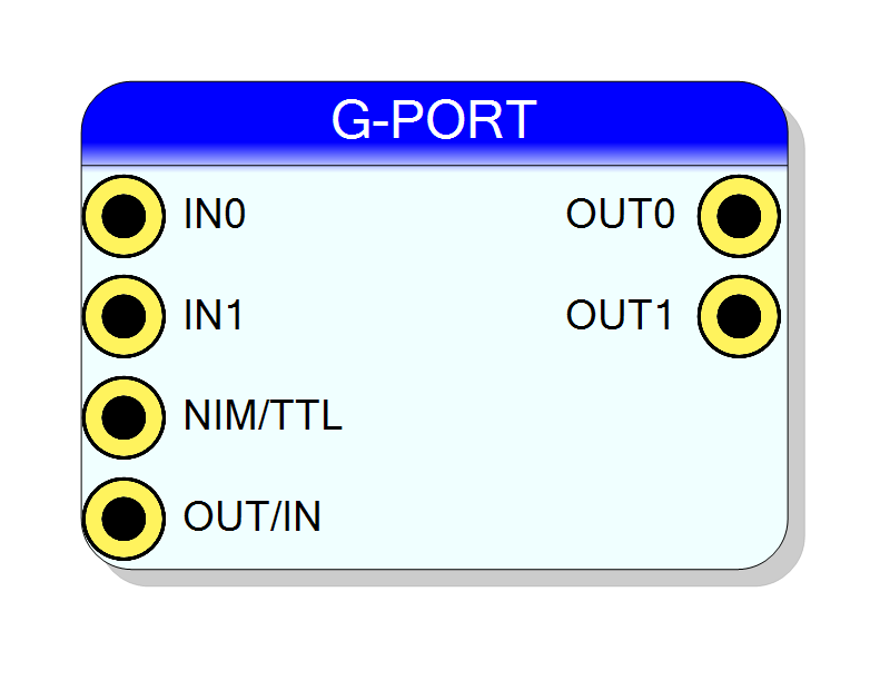
2-channel bidirectional NIM/TTL I/O port for V2495 front panel. Each channel can be independently configured as input or output with selectable signal levels.
Introduction
The G-PORT block provides access to the V2495’s 2 bidirectional front panel I/O channels. Each channel can be configured as input or output, with selectable NIM or TTL signal levels.
These are dedicated front panel connectors on the V2495, separate from the expansion slot interfaces.
Pin Description
Input signals from FPGA logic (2 channels). When configured as output (OUT/IN = 0), these values are driven to the front panel.
When using mixed mode, force unused input channels to LOW.
Output signals to FPGA logic (2 channels). When configured as input (OUT/IN = 1), these provide the signals from the front panel.
In output mode, these reflect the INx values.
Signal level selection for both channels.
- LOW (0): NIM signal levels
- HIGH (1): TTL signal levels
Direction control for both channels.
- LOW (0): Channels are outputs (INx → front panel)
- HIGH (1): Channels are inputs (front panel → OUTx)
Properties
Usage
Bidirectional Operation
Each G-PORT channel can operate as input or output:
┌──────────────────────────────────────────────────────────────────┐
│ G-PORT Signal Flow │
│ │
│ ┌─────────────┐ ┌─────────────┐ │
│ │ FPGA │═══► IN0,IN1 ════►│ │ │
│ │ Logic │ │ G-PORT │◄══► Front │
│ │ │◄══ OUT0,OUT1 ◄═══│ (2 ch) │ Panel │
│ │ │═══► OUT/IN ─────►│ │ │
│ │ │═══► NIM/TTL ────►│ │ │
│ └─────────────┘ └─────────────┘ │
└──────────────────────────────────────────────────────────────────┘
Direction Control (OUT/IN)
The OUT/IN signal controls the direction of both channels:
| OUT/IN State | Channel Direction |
|---|---|
| LOW (0) | Channels are OUTPUTS (FPGA → front panel) |
| HIGH (1) | Channels are INPUTS (front panel → FPGA) |
Note: Both channels share the same direction control.
Signal Level Selection (NIM/TTL)
The NIM/TTL signal selects the electrical standard for both channels:
| NIM/TTL State | Signal Type |
|---|---|
| LOW (0) | NIM (negative logic) |
| HIGH (1) | TTL (positive logic) |
Using Mixed Input/Output
To use one G-PORT as input and the other as output:
- Set OUT/IN to LOW (output mode)
- Force the INx pin of the input channel to LOW
- Use the OUTx pin to read the input channel
┌─────────────┐
│ Example │
│ │
│ '0' ──────►│ IN0 (unused, held low)
│ │
│ Logic ────►│ IN1 (driving output)
│ │
│ ◄─── Data ─│ OUT0 (reading input)
│ │
│ OUT/IN='0' │
└─────────────┘
Timing Diagram
Resources & Timing
-
Latency: Minimal (I/O buffer delay only)
-
Throughput: 2 bidirectional channels at FPGA clock rate
- Fixed front panel location on V2495
- Shared direction control for both channels
- Shared NIM/TTL selection for both channels
Supported Boards
- V2495