
Signed/Unsigned Converter [TM]
Time-multiplexed version of the signed/unsigned converter. Converts between signed and unsigned binary representations with configurable bit width scaling across all TM phases simultaneously. Supports four conversion modes with TM factors from 2 to 32. Pure combinational logic with zero latency.
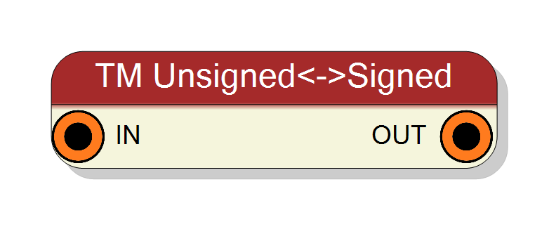
Introduction
This block is the time-multiplexed (TM) version of the signed/unsigned converter. It processes multiple parallel data streams (TM phases) in a single clock cycle, converting between signed and unsigned representations.
The operation is purely combinational with zero clock latency. Each TM phase is converted independently using the same configuration. For detailed information about conversion modes and signedness handling, see the Signed/Unsigned Converter documentation.
$$ \mathrm{OUT}_i = \mathrm{Convert}(\mathrm{IN}_i), \quad i = 0 \ldots \mathrm{TM_FACTOR} - 1 $$
Pin Description
Output TM binary signal, always TM (same factor as IN). Width per phase: Out bits property (2 to 2048 bits per phase) Total bus width: Out bits × TM Factor Interpretation: Output sign property (UNSIGNED or SIGNED)
Output is combinational (zero latency). All TM phases are converted in parallel.
Properties
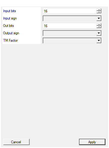
Set the number of bits of the input (per TM phase)
Number of bits per TM phase in the input signal (2 to 2048 bits). Total input width = Input bits × TM Factor.Default: 16
Range: 2 – 2048
Select the sign/unsign of the input
Interpretation of input signal (applies to all TM phases): UNSIGNED (0 to 2^N-1) or SIGNED (two’s complement, -2^(N-1) to 2^(N-1)-1).Default: UNSIGNED
Options: UNSIGNED SIGNED
Set the number of bits of the output (per TM phase)
Number of bits per TM phase in the output signal (2 to 2048 bits). Total output width = Out bits × TM Factor.Default: 16
Range: 2 – 2048
Select the sign/unsign of the output
Interpretation of output signal (applies to all TM phases): UNSIGNED (0 to 2^N-1) or SIGNED (two’s complement, -2^(N-1) to 2^(N-1)-1).Default: UNSIGNED
Options: UNSIGNED SIGNED
Select the TM Factor of the input/output
Time-multiplexing factor (number of parallel phases). Allowed values: 2, 4, 8, 16, 32. Higher values increase throughput proportionally but consume more FPGA resources (one converter instance per TM phase).Default: 4
Options: 2 4 8 16 32
Functional description
The component implements N parallel instances (where N = TM Factor) of the signed/unsigned converter. Each TM phase undergoes the same conversion operation independently:
For each phase $i$ (where $i = 0$ to TM_FACTOR - 1): $$ y[i] = \mathrm{Convert}(x[i]) $$
where the conversion mode is determined by the Input sign and Output sign properties.
TM bus structure
Time-multiplexed signals are concatenated vectors:
-
Input bus: $\mathrm{IN}[N_\text{in} \times \mathrm{TM} - 1 : 0]$
- Phase 0: bits $[N_\text{in} - 1 : 0]$
- Phase 1: bits $[2 \times N_\text{in} - 1 : N_\text{in}]$
- Phase $i$: bits $[(i+1) \times N_\text{in} - 1 : i \times N_\text{in}]$
-
Output bus: $\mathrm{OUT}[N_\text{out} \times \mathrm{TM} - 1 : 0]$
- Phase 0: bits $[N_\text{out} - 1 : 0]$
- Phase 1: bits $[2 \times N_\text{out} - 1 : N_\text{out}]$
- Phase $i$: bits $[(i+1) \times N_\text{out} - 1 : i \times N_\text{out}]$
Conversion modes (same as non-TM version)
Four conversion modes are supported (applied to all TM phases):
- Unsigned → Unsigned: Bit width change with zero extension/truncation
- Signed → Signed: Bit width change with sign extension/truncation
- Unsigned → Signed: Reinterpret as signed (add sign bit)
- Signed → Unsigned: Reinterpret as unsigned (remove sign bit)
For detailed conversion formulas and examples, refer to the Signed/Unsigned Converter documentation.
Example with TM Factor = 4
Input: 8-bit UNSIGNED to 16-bit SIGNED conversion
- Phase 0: IN = 0x7F → OUT = 0x007F (127)
- Phase 1: IN = 0xFF → OUT = 0x00FF (255)
- Phase 2: IN = 0x00 → OUT = 0x0000 (0)
- Phase 3: IN = 0x80 → OUT = 0x0080 (128)
All conversions happen in parallel within the same clock cycle.
Timing
The component is purely combinational with zero latency:
| Property | Latency (clock cycles) |
|---|---|
| Signed/Unsigned Conv TM | 0 |
All TM phases are processed in parallel within the same clock cycle.
Typical use cases
- Converting multi-channel ADC outputs (unsigned) to signed
- Interfacing TM components with different signedness requirements
- Parallel bit width adjustment for TM data streams
- Removing DC offsets from TM signals
Important notes
- All TM phases use the same conversion configuration
- Each phase is converted independently (no cross-phase interaction)
- For conversion mode details, see Signed/Unsigned Converter
- Truncation can cause overflow in individual phases