
Float LN TM
Time-multiplexed natural logarithm operator for IEEE 754 floating-point numbers based on Xilinx Floating Point IP. Supports single (32-bit) and double (64-bit) precision, configurable DSP usage, and multiple TM phases (1-32) for high-throughput parallel computation in scientific and signal processing applications.
Introduction
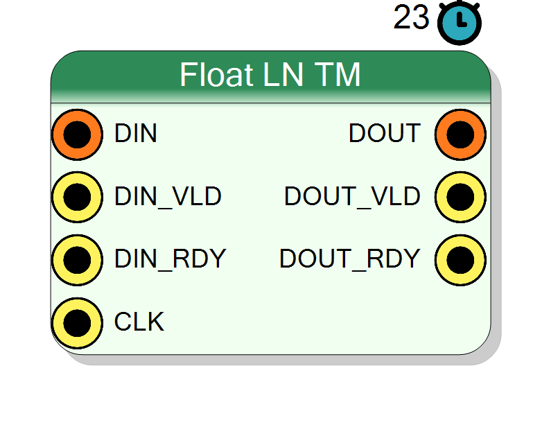
This block computes the natural logarithm (ln) of IEEE 754 floating-point values using the Xilinx Floating Point IP core. The component supports Time Multiplexing (TM): multiple parallel computation units (phases) share the same clock cycle, enabling high sample rates with predictable latency.
On every rising edge of CLK, if DIN_VLD = 1 and DOUT_RDY = 1, the operator performs
$$ \mathrm{DOUT}(n) = \ln\bigl(\mathrm{DIN}(n)\bigr), $$
where both input and output are IEEE 754 floating-point values. The TM Factor property determines how many parallel instances are instantiated.
Pin Description
Floating-point input data, always TM.
Width: (Exponent + Mantissa) × TMFactor
- Single: 32 bits/phase → total 32×TMFactor
- Double: 64 bits/phase → total 64×TMFactor IEEE 754 format input for logarithm computation. Must be positive (x > 0); negative values return NaN.
DIN_VLD = 0 the pipeline is stalled.
Maps to s_axis_a_tvalid in the AXI Stream interface.
s_axis_a_tready signals.
m_axis_result_tvalid signals.
m_axis_result_tready. Default: ‘1’ if not connected.
Properties
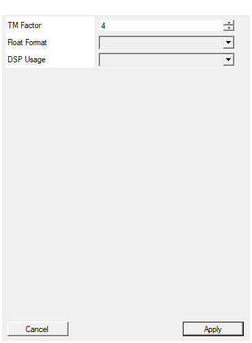
Time Multiplexing factor (number of phases)
Number of time-multiplexed phases (parallel computation units). Range: 1 – 32. Higher values increase throughput proportionally but consume more FPGA resources (N instances of the Xilinx IP).Default: 4
Range: 1 – 32
Select between single precision 32 bit and double precision 64 bit
Floating-point format for both input and output:
Single→ IEEE 754 single precision (32-bit): 8 exp + 24 mantissaDouble→ IEEE 754 double precision (64-bit): 11 exp + 53 mantissa
Determines precision and range of the computation.
Default: Single
Options: Single Double
DSP Usage. Single precision: No [0], Medium [4], Full[13]. Double precision: No[0], Medium [23], Full[61]
DSP slice usage mode:
No_Usage→ Minimize DSP usage (more LUTs)Medium_Usage→ Balanced DSP/LUT usageFull_Usage→ Maximize DSP usage (fewer LUTs)
Single precision DSP count: No [0], Medium [4], Full[13] Double precision DSP count: No[0], Medium [23], Full[61]
Default: Medium_Usage
Options: No_Usage Medium_Usage Full_Usage
Functional description
The component wraps the Xilinx Floating Point IP (operation type: Logarithm)
and replicates it N times (where N = TM Factor) to support time-multiplexed
data streams.
Input and Output
- Input
DINis always TM, with width(Exponent + Mantissa) × TMFactor - Output
DOUTis always TM, with the same width as input - Both maintain the selected precision (Single or Double)
Data valid and ready handshake
DIN_VLD(input): Input data valid, controls all phases togetherDOUT_VLD(output): Output data valid, asserted when all phases have valid outputDIN_RDY(output): Ready to accept new input (AND of all phase ready signals)DOUT_RDY(input): Downstream ready signal
Mathematical background
The natural logarithm is computed for positive real numbers:
$$ y = \ln(x) = \log_e(x) $$
Special cases:
- $\ln(1) = 0$
- $\ln(e) = 1$
- $\ln(x) \rightarrow -\infty$ as $x \rightarrow 0^+$
- $\ln(x)$ is undefined for $x \leq 0$ (returns NaN)
Properties:
- $\ln(xy) = \ln(x) + \ln(y)$
- $\ln(x^p) = p \cdot \ln(x)$
- $\frac{d}{dx}\ln(x) = \frac{1}{x}$
Timing
The Xilinx Floating Point IP has a fixed latency of 23 clock cycles per phase:
| Property | Latency (clock cycles) |
|---|---|
| Logarithm (LN) | 23 |
Total system delay: T_delay = 23 × T_CLK.
In TM mode, all phases operate in parallel with the same latency, producing
TMFactor outputs per cycle after the initial pipeline fill.
DSP Usage
The logarithm operation can be implemented with different DSP slice usage:
- Single precision: No [0], Medium [4], Full[13]
- Double precision: No[0], Medium [23], Full[61]
Higher DSP usage typically provides better performance but consumes more FPGA resources.
Typical use cases
- Signal magnitude computation in logarithmic scale
- Shannon entropy calculations
- Information theory applications
- Audio processing (dB conversions)
- Statistical analysis and machine learning
Waveform example
Example with TM Factor = 4, Single precision.
Note: 23 clock cycles of latency from input to output.