
D Latch [TM]
Time-multiplexed D-type latch for storing multiple parallel data streams. Level-sensitive transparent latch that processes 2-32 independent data phases per clock cycle. When clock enable is active, each TM phase transparently passes through; when disabled, each phase holds its value independently. Supports configurable clock edge polarity and reset values.
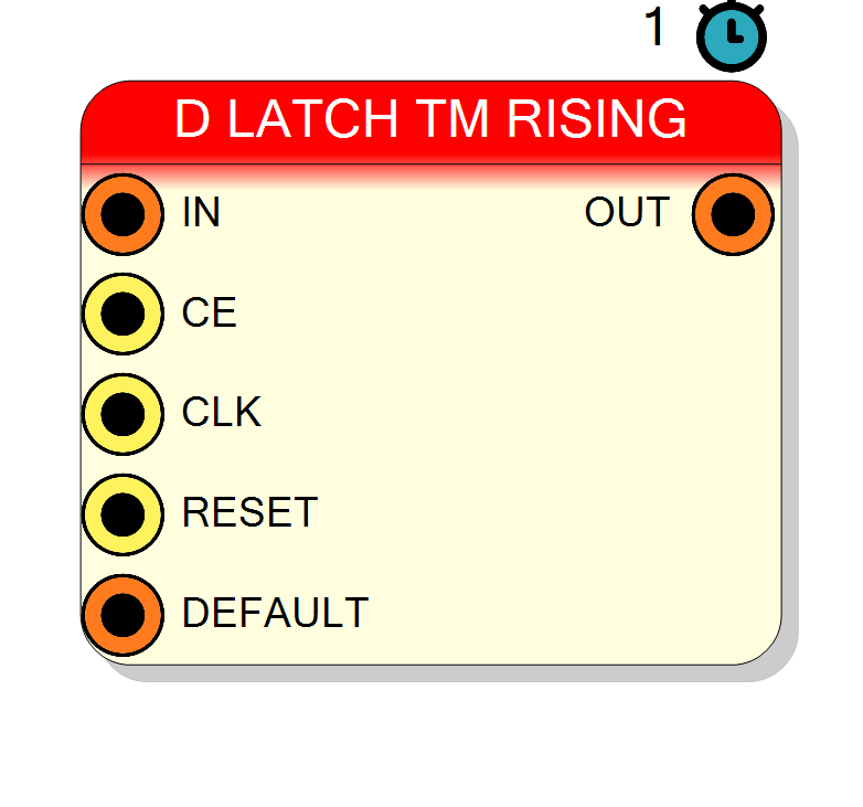
Introduction
This block implements a time-multiplexed D-type latch that processes multiple independent data streams in parallel. Each TM phase has its own latch, operating synchronously.
The TM latch operates as follows:
- When CE (clock enable) is HIGH: Output[i] = Input[i] for each phase i (transparent)
- When CE is inactive: Each Output[i] holds its previous value independently
Key characteristics:
- Level-sensitive behavior for all TM phases
- Processes 2-32 parallel data streams per clock cycle
- Each TM phase is an independent latch
- Configurable clock edge polarity (rising or falling)
- Synchronous reset with configurable default values per phase
- Latency: 1 clock cycle for all phases
Pin Description
Input Size × TM Factor
Contains TM Factor independent data values, one per phase.
Each phase is captured independently when CE is active.
Clock Enable input (active high), shared by all TM phases.
- CE = ‘1’: All latches enabled (transparent mode)
- CE = ‘0’: All latches hold their previous values Default: ‘1’ if left unconnected.
Input Size × TM Factor
Each TM phase has its own reset value, applied when RESET is asserted.
Input Size × TM Factor
Each phase reflects its independently stored value.
Latency: 1 clock cycle from input to output for all phases.
Properties
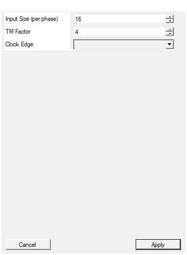
Set the number of bits per phase
Number of bits per input sample (per TM phase). Range: 1-128 bits. Total IN/OUT width = Input Size × TM Factor.Default: 16
Range: 1 – 128
Set the time multiplexing factor (number of phases)
Time-multiplexing factor (number of parallel phases). Allowed values: 2, 4, 8, 16, 32. Higher values increase throughput but consume more FPGA resources (one latch per phase per bit).Default: 4
Range: 2 – 32
Select between rising and falling edge
Clock edge polarity: RISING (latch operates on rising edges) or FALLING (latch operates on falling edges).Default: RISING
Options: RISING FALLING
Functional description
The component implements N parallel D latches (where N = TM Factor), one for each time-multiplexed phase. All latches operate synchronously on the same clock.
For each TM phase $i$ (where $i = 0$ to $N-1$):
$$ \mathrm{OUT}i = \begin{cases} \mathrm{DEFAULT}[i] & \text{if RESET = ‘1’} \ \mathrm{IN}[i] & \text{if CE = ‘1’ and RESET = ‘0’} \ \mathrm{OUT}i & \text{if CE = ‘0’ and RESET = ‘0’} \end{cases} $$
Time multiplexing architecture
The TM Factor determines how many parallel data streams are processed:
- TM Factor = 2: Two independent latches (phases 0 and 1)
- TM Factor = 4: Four independent latches (phases 0-3)
- TM Factor = 32: Thirty-two independent latches (phases 0-31)
Each phase operates independently but shares the same control signals (CLK, CE, RESET).
Truth table (Rising Edge mode)
For each TM phase:
| CLK | CE | RESET | Behavior |
|---|---|---|---|
| X | X | 1 | OUT[i] = DEFAULT[i] |
| ↑ | 1 | 0 | OUT[i] = IN[i] (transparent) |
| ↑ | 0 | 0 | OUT[i] = OUTi |
Pin width calculation
- IN width: Input Size × TM Factor
- DEFAULT width: Input Size × TM Factor
- OUT width: Input Size × TM Factor
Example: Input Size = 16, TM Factor = 4
- IN[63:0]: Four 16-bit values [IN3, IN2, IN1, IN0]
- OUT[63:0]: Four 16-bit values [OUT3, OUT2, OUT1, OUT0]
Timing
| Property | Latency (clock cycles) |
|---|---|
| D Latch TM | 1 |
All TM phases update simultaneously, one clock cycle after sampling.
TM phase mapping
The bit layout for TM signals follows this pattern:
- Phase 0: bits [(Input Size × 1) - 1 : (Input Size × 0)]
- Phase 1: bits [(Input Size × 2) - 1 : (Input Size × 1)]
- Phase i: bits [(Input Size × (i+1)) - 1 : (Input Size × i)]
- Phase N-1: bits [(Input Size × N) - 1 : (Input Size × (N-1))]
Typical use cases
- Multi-channel data storage in time-multiplexed systems
- Parallel processing pipelines with shared control
- High-throughput latch-based storage
- Sample-and-hold for multiple analog channels
- Time-division multiplexed communication systems
Design considerations
Resource utilization: The component instantiates TM Factor independent latches:
- TM Factor = 2: Uses 2× resources of single latch
- TM Factor = 32: Uses 32× resources of single latch
Timing: All phases share the same clock, so they:
- Sample simultaneously
- Update simultaneously
- Have identical latency characteristics
Warning: Like all latches, this component is level-sensitive and can introduce timing hazards. Prefer flip-flops for synchronous designs unless latches are specifically required.
Waveform example
Example with Input Size = 8, TM Factor = 4, Rising Edge, CE = ‘1’:
All four TM phases update simultaneously with one clock cycle latency.