
DT5771 Digitizer
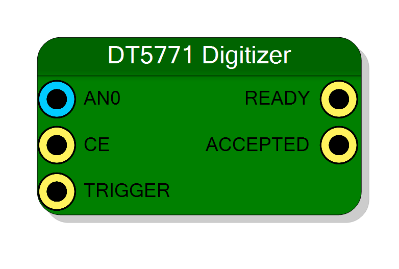
Board-pin bridge between a SciCompiler design and the digitizer engine built into the DT5771 / DT5571 board support core. It hands a 16-bit sample stream, a clock-enable and an external trigger to the board firmware, and brings back the engine’s READY and EVENT_ACCEPTED status lines. It contains no logic of its own.
Introduction
Principle of Operation
The DT5771 and DT5571 carry a fixed board support core (DESIGN_TOP) that
already implements the acquisition back end: event buffering, the Avalon
memory-mapped interface to the host, the front-panel and display logic. That
core exposes four signals to the user design, and this block is the named
access point to them.
The block is a thin wrapper: it generates no entity, no generic and no
VHDL file. CompileHDL calls GenerateServiceHDL and then emits five
plain concurrent assignments:
DIGITIZER_CH0 <= <net of AN0>; -- 16-bit sample stream
DIGITIZER_CE <= <net of CE>; -- clock enable / sample valid
DIGITIZER_EXT_TRIGGER <= <net of TRIGGER>; -- external trigger
<net of ACCEPTED> <= DIGITIZER_EVENT_ACCEPTED; -- only if connected
<net of READY> <= DIGITIZER_READY; -- only if connected
The four DIGITIZER_* names are top-level signals of the board wrapper
(support_files/dt5771_dll/.../top_project_name.vhd), wired straight to the
DIGITIZER_CH0, DIGITIZER_CE, EXT_TRIGGER, DIGITIZER_READY and
DIGITIZER_EVENT_ACCEPTED ports of the DESIGN_TOP component.
Where it sits in a design
board ADC ──► (ADC input block) ──► your processing chain ──► ┌──────────────────┐
│ DT5771 Digitizer│
trigger logic ────────────────────────────────────────────────►│ TRIGGER READY │──► status
sample-valid ─────────────────────────────────────────────────►│ CE ACCEPTED │──► status
└────────┬─────────┘
│
board support core (DESIGN_TOP)
→ event buffer → host
Note the direction: AN0 is a symbol input. The block takes a waveform
from the design and gives it to the board’s digitizer engine - it is the
point at which a processed signal re-enters the standard DT5771 acquisition
path, not a source of ADC samples.
Pin Description
DIGITIZER_CH0. This is the waveform
the board firmware will digitize and buffer, so it is where your
processing chain (filter, shaper, gain stage, or just the raw ADC block)
ends. Left unconnected it is tied to x"0000", i.e. a flat zero trace.
DIGITIZER_CE. Assert it
on the cycles where AN0 carries a new sample; deassert it to decimate
the stream or to stall the engine while your chain has no valid output.
Left unconnected it is tied to '1', so every clock cycle is taken as a
valid sample.
EXT_TRIGGER port. Drive it from your own discriminator, coincidence or
software-pulse logic to make the board record an event on your condition
rather than on its internal one. Left unconnected it is tied to '0'
and never fires.
DIGITIZER_READY status line.
The assignment is emitted only when the pin is connected, so leaving it
open costs nothing. Not available on the MINIMAL FPGA variant - see the
alert in the description.
DIGITIZER_EVENT_ACCEPTED
status line, telling the design that the engine has taken an event.
Useful as a dead-time or acceptance-rate indicator. Emitted only when
connected, and not available on the MINIMAL FPGA variant.
⚙️ Detailed Operation
What the block does, exactly
Everything the component contributes is in the five assignments above. Concretely that means:
- No latency, no registers. The pins are aliases; a value present on
AN0in clock cycle n is onDIGITIZER_CH0in the same cycle. - No properties. The property list is empty, so double-clicking the block shows nothing to configure. Everything about how the event is built, triggered, buffered and read is configured on the board side (the DT5771 configuration dialog and the host software), not here.
- No registers and no SciSDK code.
CompileMMCandCompileSDKboth returnTruewithout emitting anything: this block creates no endpoint. The host talks to the digitizer through the board’s own interface. - No compile-time validation. The only message it prints is the
informational
Generating HDL code for <designator>.
Default connections
Each input carries a default that is pasted into the assignment when the pin is left unconnected, so a partially wired block still compiles and behaves sensibly:
| Pin | Value when left open | Effect |
|---|---|---|
AN0 |
x"0000" |
a flat zero waveform is sent to the engine |
TRIGGER |
"0" |
the external trigger is never asserted |
CE |
"1" |
every clock cycle carries a valid sample |
The two outputs are different: they are emitted only if connected. The
generator tests __Con <> "open" before writing the assignment, so an
unconnected READY or ACCEPTED produces no line at all.
One instance per design
The assignments to DIGITIZER_CH0, DIGITIZER_CE and
DIGITIZER_EXT_TRIGGER are unconditional concurrent statements on top-level
signals.
Supported boards
The component is bound by GUID to exactly two boards:
| Board GUID | Board |
|---|---|
4AE1FD38-74D1-4E29-BAC4-C45776E4BA75 |
DT5771 |
B056EB81-48BF-4F3E-B910-3BFD0AA50A89 |
DT5571 |
It does not appear in the palette for any other target. The two boards carry
the same DIGITIZER_* interface, which is why one component serves both.
What is not documented here
The behaviour behind the interface - when READY rises, exactly what
EVENT_ACCEPTED pulses on, how the trigger is qualified, the event format
delivered to the host and the registers that configure it - lives inside the
board support core, which is distributed as a pre-built netlist. None of it
can be established from this plug-in’s sources, so nothing is claimed about it
here. Treat READY and ACCEPTED as status indications from the board
firmware and refer to the DT5771 / DT5571 board documentation for their exact
timing.
Resources & Timing
- Latency: 0 clock cycles - the block emits concurrent assignments only, with no register stage in either direction.
- No generics, no
.vhdresource, no HLS core and no memory-mapped registers are produced by this block. - The component declares no properties at all, so it has no property dialog.