
Averaged Oscilloscope
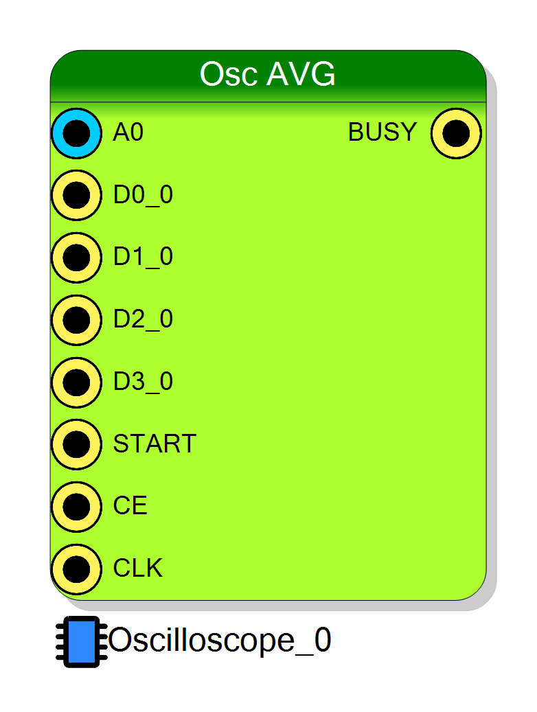
Oscilloscope Averaged is a multi–channel oscilloscope IP core for Xilinx-7 devices able to acquire up to 32 analog channels (16-bit each) together with 4 groups of digital lines. Compared with the standard oscilloscope, the AVG version performs an on-the-fly box-car average whenever a decimation factor CONFIG_DECIMATOR > 0 is programmed. Fast digital transitions occurring inside the decimation window are preserved thanks to an integrated peak holder, guaranteeing glitch-free mixed-signal acquisitions.
Introduction
Principle of operation
Let
- $f_s$ = input sampling frequency
- $N$ = 2^D, with D = CONFIG_DECIMATOR ∈ [0‥20]
- $x_k(i)$ = k-th raw sample of channel i
- $y_m(i)$ = m-th decimated (and possibly averaged) sample stored in RAM
When $D = 0$ the core behaves exactly as the standard oscilloscope: $y_m(i) = x_m(i)$.
For $D > 0$ the core computes the arithmetic mean of $N = 2^D$ consecutive raw samples:
$$ y_m(i)=\frac{1}{N}\sum_{k=0}^{N-1}x_{mN+k}(i) $$
The implementation uses an accumulator that grows
$Wordsize + D$ bits. When the free-running decimation counter reaches 0
(counterDecimator = 0) the accumulator is right-shifted by D and
cleared, yielding one averaged sample every ** $N / f_s$** seconds.
All timing-critical operations (trigger evaluation, accumulation, peak
detection and memory write) occur in the same CLK_WRITE domain, guaranteeing
deterministic behaviour.
Digital peak holder
For each digital line a bitwise OR is performed across the same N cycles:
$$ d^{PH} = \bigvee_{k=0}^{N-1} d_k $$
where $d_k$ is the instantaneous value and $d^{PH}$ is the value written in RAM ($tMemD?$). In this way even a single-clock pulse is captured inside an averaged window.
Pin Description
CONFIG_TRIGGER_MODE(2:0)=000.
CLK.
CLK_WRITE in VHDL).
READ_STATUS(2:0)="100").
Properties
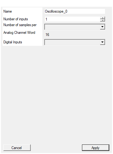
Set the name of the endpoint
Logical name of the endpoint generated in the firmware and exported to the software register map. Change only if multiple oscilloscopes are instantiated.Default: Oscilloscope_0
Set the number of input to the virtual block
Number of analog channels (1 – 32).Impacts memory depth per channel (
Samples) and resource usage because
each channel instantiates an independent dual-port RAM.
Default: 1
Range: 1 – 32
Set the number of samples stored for each acquisition
Circular buffer length per channel. Must be a power of two between 128 and 16384.Default: 1024
Options: 128 256 512 1024 2048 4096 8192 16384
Set the analog channel word size in bits
Width of each analog sample in bits (fixed to 16 bit for this core and therefore read-only).Default: 16
Range: 1 – 16
Enable/Disable Digital Inputs
Enable or disable the compilation of the 4 digital groups.Disabling saves LUTs if only analog data are required.
Default: Enabled
Options: Enabled Disabled
⚙️ Detailed Timing
Event Sequence (Overview)
- ARM (
CONFIG_ARM0→1) Clears internal counters (including the decimation counter) and puts the core into the armed state. - Raw sampling Every clock cycle (frequency $f_s$, period $T_{\text{CLK}} = 1/f_s$) with $CE=1$ the design acquires simultaneously:
- 16-bit analog samples for each enabled channel.
- Digital lines (groups D0…D3) for the peak-holder logic.
- Trigger evaluation
Performed every clock cycle according to
CONFIG_TRIGGER_MODE(externalSTART, analog threshold, software, or digital line). - Trigger time stamping
When the condition becomes true (e.g. rising edge of
START, threshold crossing, software flag), the current circular write pointer is latched as the Trigger Write Pointer (TWP). - Post-trigger writing
Continues until the buffer (
Samples) is filled (i.e. post-trigger region complete). - Acquisition end →
READ_STATUS = 1;BUSYreturns low.
Delay Between TRIG (START) and First Valid Sample
Let $D = \text{CONFIG_DECIMATOR}$ and $N = 2^{D}$. “First valid sample” = the output sample (raw if $D=0$, averaged/decimated if $D>0$) that contains (or corresponds to) the trigger time in the reconstructed waveform.
| Case | Write-path pipeline | Practical meaning |
|---|---|---|
| $D=0$ | 2 clock cycles (1 stage + RAM) | Raw sample taken on trigger cycle becomes readable after $2,T_{\text{CLK}}$. |
| $D>0$ | Finish active accumulation window + pipeline → up to $N$ cycles + 2 | Averaged sample containing trigger appears at window close: worst case $\approx (N+2)T_{\text{CLK}}$. |
The trigger acts on the instantaneous raw sample. If the trigger occurs inside an open decimation window, the averaged value is produced only when the decimation counter rolls to 0 and the accumulator is right-shifted by $D$.
Latency formulas:
$$ t_{\text{lat,min}} = 2T_{\text{CLK}} \quad (D=0) $$
$$ t_{\text{lat,avg}} \approx \left(\frac{N}{2} + 2\right)T_{\text{CLK}} \quad (D>0) $$
$$ t_{\text{lat,max}} = (N + 2)T_{\text{CLK}} \quad (D>0) $$
Pre-Trigger Mechanism
CONFIG_PRETRIGGER = P = number of output samples that must appear before the trigger point in the reordered waveform.
- If $D=0$: $P$ = number of raw samples preceding the trigger.
- If $D>0$: $P$ = number of decimated windows preceding the window that contains the trigger (raw history depth $= P N$ samples).
Full pre-trigger condition: The core must have been armed long enough so that at least $P$ output samples (windows) have been written before the trigger; otherwise effective pre-trigger is shorter.
Reordering:
Let READ_POSITION be the (unreordered) index $I_T$ of the trigger sample/window. Define
$$ \text{fix_position} = I_T - P. $$
- If $\text{fix_position} > 0$: concatenate $data[\text{fix_position}:] + data[:\text{fix_position}]$.
- If $\text{fix_position} < 0$: let $idx = \text{fix_position} + Samples$ then use $data[idx:] + data[:idx]$.
After reorder, trigger sample is at index $P$.
Example ($D=0$): $Samples = 4096$, $P=1024$, $I_T=1500$ → $\text{fix_position}=476$.
Example ($D>0$): $D=3 \Rightarrow N=8$. $P=256$ means $256$ windows = $2048$ raw samples of pre-history (time $\approx 2048/f_s$).
4. Effective Acquisition Duration Relative to Trigger
Let $Samples = S$ (total output samples). Pre-trigger output samples = $P$; post-trigger output samples = $S-P$.
For $D=0$:
$$ T_{\text{pre}} = \frac{P}{f_s}, \quad T_{\text{post}} = \frac{S-P}{f_s}, \quad T_{\text{total}} = \frac{S}{f_s}. $$
For $D>0$ (each output sample represents $N$ raw samples):
$$ T_{\text{pre}} = \frac{PN}{f_s}, \quad T_{\text{post}} = \frac{(S-P)N}{f_s}, \quad T_{\text{total}} = \frac{SN}{f_s}. $$
Trigger placement inside window ($D>0$): Trigger raw sample offset $r \in [0,N-1]$. If you time-stamp a decimated sample at the window center:
$$ t_{\text{window center}} = \left(iN + \frac{N-1}{2}\right) T_{\text{CLK}} $$
Temporal uncertainty without exporting $r$:
$$ \Delta t_{\text{max}} \approx \frac{N-1}{2} T_{\text{CLK}}. $$
Digital Peak Holder Timing
For $D>0$, each window produces one peak-held digital vector:
$$ d^{\text{PH}} = \bigvee_{k=0}^{N-1} d_k $$
It is emitted alongside the averaged analog sample and shares the same worst-case latency $(N+2)T_{\text{CLK}}$. Single-cycle pulses are captured; frequent toggling may keep bits high.
Quick Reference
| Parameter | Formula / Meaning |
|---|---|
| Decimation factor | $N = 2^D$ |
| Min latency ($D=0$) | $2T_{\text{CLK}}$ |
| Max latency ($D>0$) | $(N + 2)T_{\text{CLK}}$ |
| Pre-trigger time | $P/f_s$ ($D=0$); $(PN)/f_s$ ($D>0$) |
| Post-trigger time | $(S-P)/f_s$ ($D=0$); $((S-P)N)/f_s$ ($D>0$) |
| Total acquisition time | $S/f_s$ ($D=0$); $(SN)/f_s$ ($D>0$) |
| Trigger timing uncertainty ($D>0$) | $\le \frac{N-1}{2} T_{\text{CLK}}$ |
Oscilloscope Configuration Registers
CONFIG_ARM
- A rising edge (0 → 1) on this register enables the oscilloscope acquisition.
- It acts as a trigger arm: write
0, then1to activate.
CONFIG_DECIMATOR
- Sets the decimation factor for the output data.
- A value of
0disables decimation; higher values reduce the sampling rate accordingly.
CONFIG_TRIGGER_MODE
- Defines the trigger mode and its associated parameters:
| Bits | Purpose | Description |
|---|---|---|
| 0–2 | Trigger Source | 000 → External trigger001 → Analog signal010 → Software trigger100 to 111 → Digital inputs 0–3 |
| 3 | Trigger Edge (Analog mode only) | 0 → Rising edge1 → Falling edge |
| 6 | Software Trigger | Set to 1 to trigger immediately when in software mode |
| 8–15 | Channel Selection (Analog/Digital modes) | Selects which channel to monitor |
CONFIG_PRETRIGGER
- Sets the number of pre-trigger samples, i.e., how far back in time the waveform capture should begin relative to the trigger event.
CONFIG_TRIGGER_LEVEL
- Specifies the trigger threshold level (in LSB) used for analog signal triggering.
READ_STATUS
-
Indicates data availability:
0→ Data not ready1→ Data available for reading
READ_POSITION
- Provides the sample index of the trigger within the captured data buffer.
Reading Waveform Data
Once data is ready (READ_STATUS = 1), waveform samples can be retrieved by reading from the oscilloscope’s data address (defined in the JSON descriptor). The number of samples is equal to the configured nsamples.
🌀 Data Reordering and Circular Buffer Handling
After acquisition, data must be reordered so the trigger event always appears at the same position in the waveform, defined by CONFIG_PRETRIGGER.
Two scenarios are possible:
1. Trigger after the pre-trigger index
-
fix_position > 0 -
Reconstruct data as:
reordered_data = data[fix_position : ] + data[ : fix_position]
2. Trigger before the pre-trigger index (wrap-around)
-
fix_position < 0 -
Use circular indexing:
idx = fix_position + nsamples reordered_data = data[idx : ] + data[ : idx]
This ensures consistent waveform alignment for analysis and visualization.