
D Flip-Flop (Falling Edge)
Falling-edge-triggered D-type flip-flop for synchronous data storage. Samples multi-bit input data on falling clock edges and provides stable registered output. Supports clock enable control, synchronous reset with configurable preset values, and prevents timing hazards through edge-triggered operation.
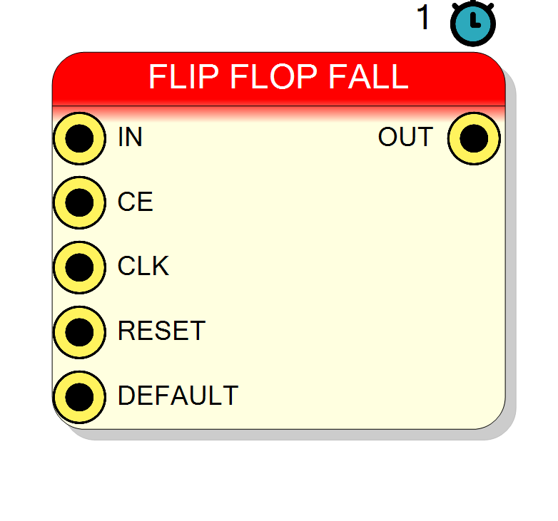
Introduction
This block implements a D-type flip-flop that captures data on falling clock edges. Unlike level-sensitive latches, flip-flops are edge-triggered, providing clean timing isolation between input and output.
The flip-flop operates as follows:
- On falling clock edge (↓) with CE = ‘1’: Output = Input
- Between clock edges: Output holds its value (input changes are ignored)
Key characteristics:
- Edge-triggered operation (samples only on falling edges)
- Clock enable for conditional updates
- Synchronous reset with configurable preset value
- Latency: 1 clock cycle
- Useful for dual-edge systems or phase-shifted designs
Pin Description
Clock Enable input (active high).
- CE = ‘1’: Flip-flop samples IN on falling edges
- CE = ‘0’: Flip-flop holds current OUT value Default: ‘1’ if left unconnected.
Properties
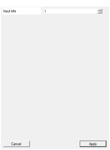
Set the number of bits of the input
Number of bits in the flip-flop (width of IN, DEFAULT, and OUT). Range: 1-2048 bits.Default: 1
Range: 1 – 2048
Functional description
A falling-edge D flip-flop captures its input value only at falling (high-to-low) clock transitions. This component implements the following behavior:
Truth table
| CLK | CE | RESET | Behavior |
|---|---|---|---|
| X | X | 1 | OUT = PRESET (next ↓) |
| ↓ | 1 | 0 | OUT = IN |
| ↓ | 0 | 0 | OUT = OUT(previous) |
| ↑,— | X | 0 | OUT = OUT(previous) |
Edge-triggered sampling
The flip-flop samples its input only at the falling edge of the clock:
- Input is captured precisely at the high-to-low clock transition
- Changes on IN between clock edges have no effect
- Provides timing isolation: input and output are separated by a register stage
Clock enable operation
The CE (Clock Enable) input allows conditional updates:
- CE = ‘1’: Flip-flop captures new data on falling edges
- CE = ‘0’: Flip-flop holds current value (input ignored)
Reset and preset
The component supports synchronous reset:
- When RESET = ‘1’: Output is set to the PRESET value on the next falling clock edge
- PRESET input defines the reset state (can be any value)
- Reset is synchronous: requires a clock edge to take effect
Falling edge vs Rising edge
Falling-edge flip-flops:
- Sample on ↓ (high-to-low) transitions
- Useful for:
- Dual-edge systems (double throughput)
- Phase-shifted timing alignment
- Interface with falling-edge devices
Rising-edge flip-flops:
- Sample on ↑ (low-to-high) transitions
- More common in modern designs
- Standard convention in most digital systems
Both types provide the same storage functionality, just with different clock phasing.
Timing
| Property | Latency (clock cycles) |
|---|---|
| D Flip-Flop Falling | 1 |
The output updates exactly one clock cycle after the input is sampled.
Typical use cases
- Dual-edge systems: Combine with rising-edge FFs for double data rate (DDR)
- Phase-shifted pipelines: Aligning data with inverted clock phases
- Interface logic: Connecting to devices that use falling-edge clocking
- Clock domain crossing: Sampling on opposite edge from source domain
- Timing alignment: Adjusting data phase by half a clock cycle
- DDR interfaces: Data capture on both clock edges
Design considerations
- Clock polarity: Ensure clock signal has correct polarity for intended operation
- Setup/hold: Falling edge timing is equivalent to rising edge (just inverted clock)
- Mixing edges: Carefully manage timing when mixing rising and falling edge logic
- DDR systems: Use both rising and falling edge FFs for double data rate designs
- Reset timing: Reset operates on falling edges (may differ from rising-edge conventions)
Waveform example
Example with Input Size = 8 bits, showing falling-edge-triggered operation:
Note:
- At falling edge: OUT = A (sampled on ↓, CE = 1)
- CE = 0 during middle: B is ignored (CE = 0)
- At next falling edge: OUT = C (sampled on ↓, CE = 1)