
Accumulator Simple (TM)
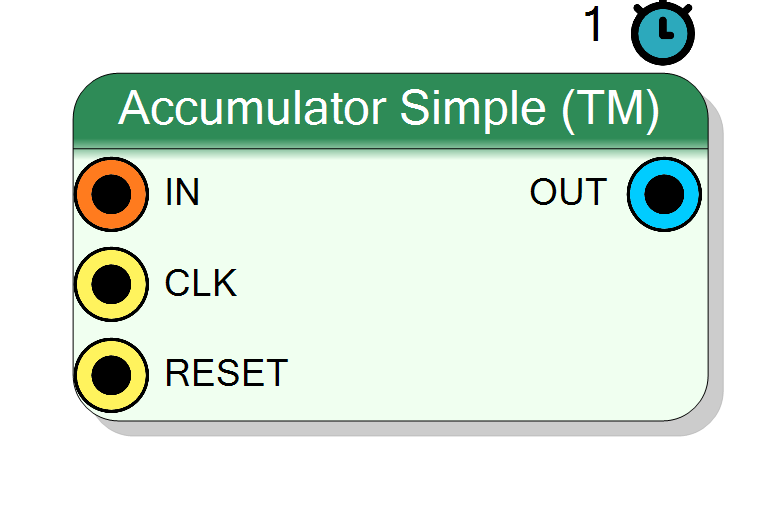
Time-multiplexed accumulator that sums all TM phases into a single scalar output. Accepts TM input (2-32 phases) and produces non-TM accumulated sum. Configurable accumulator bit width (8-64 bits) and input width (4-32 bits). Implemented using Xilinx HLS with 1 clock cycle latency.
Introduction
This block sums all TM phases together into a single accumulator, producing a scalar (non-TM) output. Unlike Accumulator Full which maintains N independent accumulators, this variant performs a reduction operation.
On every rising edge of CLK, the single accumulator updates:
$$ \mathrm{OUT}[n] = \mathrm{OUT}[n-1] + \sum_{i=0}^{N-1} \mathrm{IN}_i[n], $$
where $N$ is the TM Factor and $\mathrm{IN}_i$ are the TM input phases.
A synchronous active-high RESET clears the accumulator to zero.
Pin Description
Input bits × TM Factor
All TM phases are summed together into the accumulator.
Accumulator bits (single value)
Contains the running sum of all input samples from all TM phases.
Valid after 1 clock cycle from input.
Properties
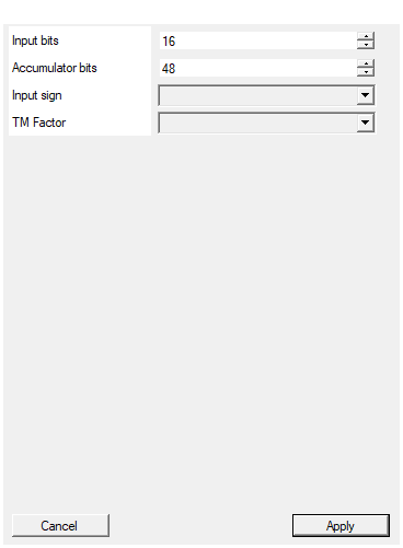
Set the number of bits of each input sample
Number of bits per input sample ($N_\text{in}$). Range: 4 – 32. Determines input dynamic range per TM phase.Default: 16
Range: 4 – 32
Set the number of bits of the accumulator output
Width of the accumulator register ($N_\text{acc}$). Range: 8 – 64. Should account for both input range and TM factor to prevent overflow.
Recommended: $N_\text{acc} \geq N_\text{in} + \log_2(\text{TM Factor}) + \text{headroom}$
Default: 48
Range: 8 – 64
Select the sign/unsign of the input
Arithmetic type of input and accumulator:
- UNSIGNED → Non-negative integers, wrap at $2^{N}-1$
- SIGNED → Two’s complement, range $[-2^{N-1}, 2^{N-1}-1]$
Accumulator preserves sign type.
Default: UNSIGNED
Options: UNSIGNED SIGNED
Select the Time Multiplexing factor (samples per word)
Number of time-multiplexed input phases to sum together. Allowed values: 2, 4, 8, 16, 32.
All TM phases are added to the same accumulator each clock cycle, effectively multiplying the accumulation rate by the TM factor.
Default: 8
Options: 2 4 8 16 32
Functional description
The component implements a TM-to-scalar reduction accumulator using Xilinx HLS. All TM input phases are summed together and added to a single accumulator register each clock cycle.
Operation
The accumulator updates according to:
$$ \text{acc}[n] = \text{acc}[n-1] + \sum_{i=0}^{N-1} x_i[n], \qquad \text{acc}[-1] = 0 $$
where:
- $x_i[n]$ →
IN(TM phases $i = 0, \ldots, N-1$) - $\text{acc}[n]$ →
OUT(single scalar value) - $N$ → TM Factor
Use case comparison
| Component | Input | Output | Accumulators | Use Case |
|---|---|---|---|---|
| Accumulator Full | TM (N ch) | TM (N ch) | N independent | Per-channel integration |
| Accumulator Simple | TM (N ch) | Scalar (1) | 1 shared | Total energy across all ch |
Accumulator width
The accumulator register width (Accumulator bits) should account for both the input dynamic range and the TM factor:
For unsigned inputs summing $N$ phases: $$ \text{Headroom} = \frac{2^{w_\text{acc}}}{N \cdot 2^{w_\text{in}}} = \frac{2^{w_\text{acc} - w_\text{in}}}{N} $$
Example: 16-bit input, TM=8, 48-bit accumulator → $2^{32}/8$ = 536M samples headroom.
Mathematical background
In the $z$-domain, the system has transfer function:
$$ H(z) = \frac{N}{1 - z^{-1}} $$
The factor of $N$ comes from summing all TM phases together each cycle. This represents a discrete-time integrator with gain N.
Timing
The HLS-generated IP has a fixed latency of 1 clock cycle:
| Property | Latency (clock cycles) |
|---|---|
| Accumulator Simple (TM) | 1 |
Total system delay: T_delay = 1 × T_CLK.
Note: This is faster than Accumulator Full (3 cycles) due to simpler logic.
Typical use cases
- Total charge/energy measurement across all channels
- Global event rate counting
- Sum of ADC values from multiple channels
- Aggregate pulse counting
- Multi-channel coincidence integration
Waveform example
Example with TM Factor = 4, Input = [1, 2, 3, 4, 1, 2, 3, 4, …].
Note: OUT = sum of all 4 phases (1+2+3+4=10, then 10+1+2+3+4=20), 1 cycle latency.