

RF Baseband DDC (SSR4)
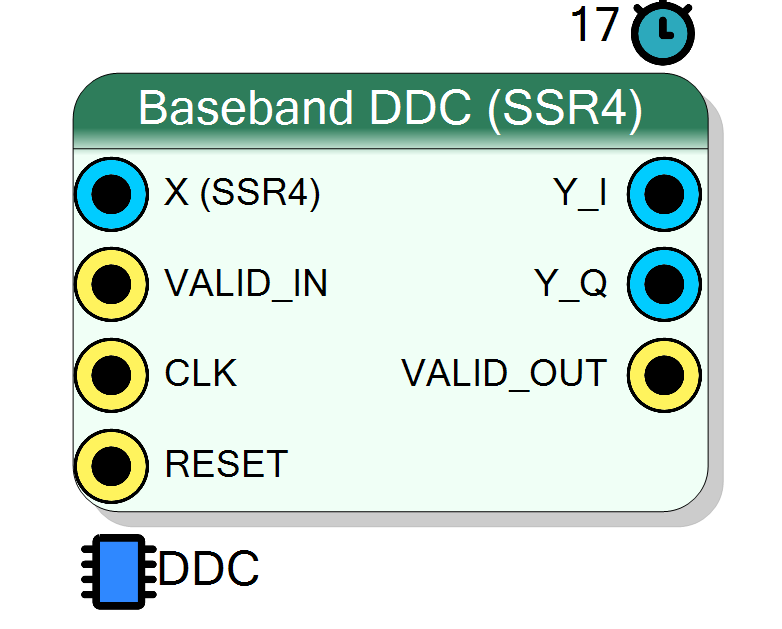
Super-sample-rate digital down-converter from the KriaTest (KR260) live DSP demo: 4 ADC samples per clock (1 GSPS at 250 MHz) are mixed by a 32-bit NCO and decimated by 4 with two half-band filters, giving one complex int16 baseband sample per clock (250 MSPS). Centre frequency is a register (PHASE_INC), retunable at run time.
Introduction
Port of the KriaTest baseband_ddc HLS block (silicon-proven on Kria
KR260). The arithmetic is byte-for-byte the KriaTest loop body; only the
control model changed: the SciCompiler block is free-running (one HLS
call per clock), gated by VALID_IN.
X (4 x int16 / clock) --+--> NCO e^-j2pi fc t (LUT 4096x18) --> mixer
| (phase_inc = round(fc/1GSPS * 2^32))
+--> HB1 15 taps /2 (500 MSPS, 2 outputs/clk)
HB2 31 taps /2 (250 MSPS, 1 output/clk)
--> Y_I / Y_Q int16, VALID_OUT
The TM twin (baseband_ddc_tm) packs several independent DDCs (one per
antenna / ADC) on one bus.
Pin Description
Properties
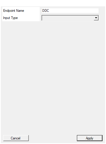
Name of the register endpoint. Registers are REG_
DDC).
Default: DDC
Real: one ADC, X = 4 x int16 lanes (KriaTest default, DDC_REAL_INPUT=1). Complex: I/Q from an external mixer, X_I and X_Q (DDC_REAL_INPUT=0).
Real (one ADC,DDC_REAL_INPUT=1, KriaTest default) or Complex
(I/Q from an external mixer, DDC_REAL_INPUT=0).
Default: Real
Options: Real Complex
Usage
Register interface (endpoint = EndpointName, KriaTest page DDC)
| register | access | meaning |
|---|---|---|
CTRL |
W | b1 clear (level: state held at zero while 1 - write 1 then 0); b0 enable is a shadow bit (no effect, as in KriaTest) |
PHASE_INC |
W | NCO increment, round(fc / 1e9 * 2^32) for a 1 GSPS input |
Net names: REG_<EP>_CTRL_WR, REG_<EP>_PHASE_INC_WR. With
EndpointName = DDC they are exactly the KriaTest names. The registers
come from the bus clock domain and are 2-FF synchronised inside the block.
Sample format
Lane k of X (or X_I / X_Q) is bits [16k+15 : 16k]; lane 0 is the
OLDEST sample of the clock (KriaTest ddc_in_t). Output: Y_I / Y_Q
signed int16 (Q1.15), saturated.
Behaviour
VALID_IN = 1: one SSR4 group consumed,VALID_OUT = 117 clocks later.VALID_IN = 0: state frozen, no output (unconnectedVALID_IN= ‘1’).CTRL.clear = 1: NCO phase and both delay lines zeroed, no output.PHASE_INCis read every clock: retuning needs no restart.
Resources & Timing
-
Latency: 17 clocks
-
Throughput: One SSR4 group (4 samples) per clock in, one complex sample per clock out
Vitis HLS 2022.2 on xck26-sfvc784-2LV-c at 4 ns: Real 38 DSP / 16 BRAM18 (NCO LUT) / ~3.6k FF / ~2.4k LUT, estimated 3.39 ns; Complex 46 DSP. Verified bit-exact against the untouched KriaTest C function, at C level and on the generated RTL in GHDL (tb/kria_ddc).