
Synchronizer (Legacy)
Legacy Xilinx-only synchronizer for multi-bit clock domain crossing. Provides single-stage synchronization between asynchronous clock domains using Xilinx-specific primitives. This is a deprecated component maintained for backwards compatibility. New designs should use the CCCC (Bit-Array Sync) component for vendor-independent, safer multi-stage synchronization.
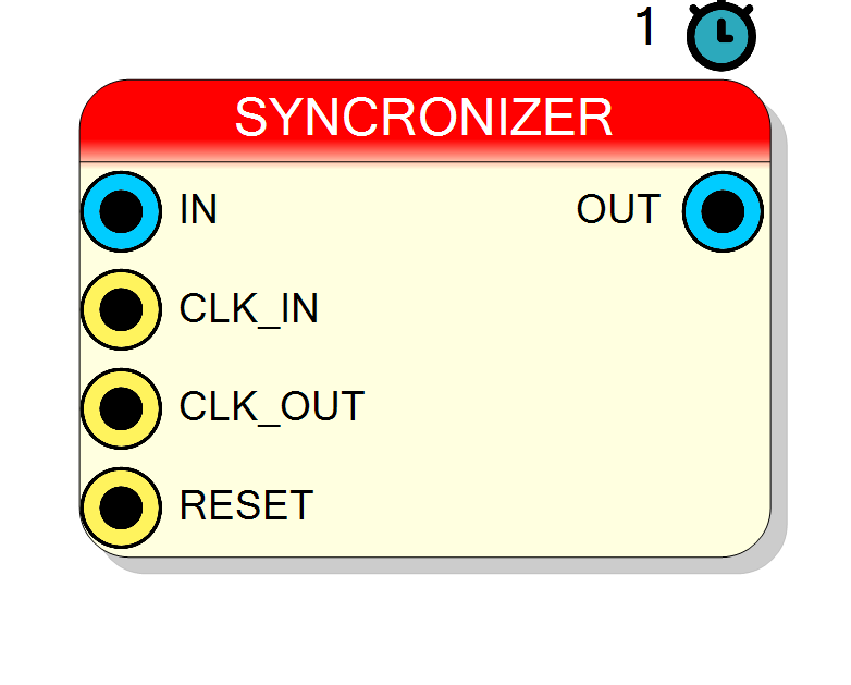
Introduction
This block implements a legacy synchronizer for transferring multi-bit data between asynchronous clock domains. This component is deprecated and retained only for backwards compatibility with existing designs.
IMPORTANT: This component:
- Uses Xilinx-specific VHDL primitives (not portable)
- Provides single-stage synchronization (less metastability protection)
- Is legacy: Replaced by CCCC component
For new designs, use CCCC (Bit-Array Sync) instead, which provides:
- Vendor-independent implementation
- Four-stage synchronization (better MTBF)
- Modern CDC best practices
Pin Description
Properties
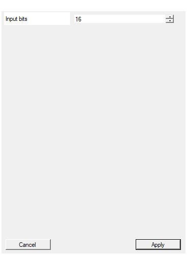
Set the number of bits of the data vector
Number of bits to synchronize (width of IN and OUT). Range: 1-1024 bits. Legacy single-stage synchronizer per bit. For new designs, use CCCC instead.Default: 16
Range: 1 – 1024
Functional description
This legacy synchronizer provides Clock Domain Crossing (CDC) functionality using a single-stage flip-flop per bit, implemented with Xilinx-specific primitives.
Single-stage synchronization
Each input bit passes through one flip-flop in the destination domain:
$$ \mathrm{OUT}[i] = \mathrm{FF}_1(\mathrm{IN}[i]) $$
Where $\mathrm{FF}_1$ is clocked by CLK_OUT.
Limitations
- Single-stage: Lower MTBF than multi-stage synchronizers
- Xilinx-only: Uses vendor-specific VHDL constructs
- Legacy architecture: Does not follow modern CDC practices
- Metastability risk: Higher probability of metastable failures
Migration path
For new designs or when updating legacy designs:
Old (this component):
Component: SYNCHRONIZER (CCCClegacy)
Stages: 1
Vendor: Xilinx only
New (recommended):
Component: Bit-Array Sync (CCCC)
Stages: 4
Vendor: Independent
Timing
| Property | Latency (CLK_OUT cycles) |
|---|---|
| Synchronizer | 1 |
The output appears 1 clock cycle (in the destination domain) after the input changes.
Note: Lower latency but higher metastability risk compared to multi-stage synchronizers.
Why this is legacy
- Insufficient stages: Modern designs use 2+ stages for adequate MTBF
- Vendor lock-in: Xilinx-specific code limits portability
- Safety: CCCC’s four-stage design provides exponentially better protection
- Standards: Industry best practices recommend multi-stage synchronizers
Typical use cases (legacy)
This component should only be used:
- In existing designs for backwards compatibility
- When migrating legacy Xilinx designs
- As a temporary placeholder during migration to CCCC
Do not use in new designs.
Waveform example
Example showing single-stage CDC:
Note: Only 1-cycle latency, but higher metastability risk.