System Sync
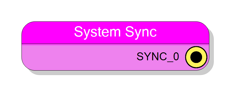
Board pin block that brings one of the three R5560 / R5560SE SYNC lines into the diagram as a 1-bit signal. The lines are LVDS receivers on the board, so the block is read-only - there is no output direction on these boards. One concurrent assignment, no register, no synchroniser.
Introduction
Principle of Operation
The R5560 and R5560SE carry three system SYNC lines. Unlike the DT5560’s single-ended SYNC pairs, these are differential LVDS and - this is the fact that shapes the whole block - they are inputs only.
In the board’s top-level design each one is received by an IBUFDS:
SYNC_n_P ──┐
├─ IBUFDS (DIFF_TERM = TRUE) ──► SYNC_n ──► your diagram
SYNC_n_N ──┘
There is no output buffer and no output port anywhere on the path, which is why this plug-in ships a System Sync block with an output pin and no counterpart that drives a SYNC line. If you need to send a sync out of an R5560, this is not the block, and nothing in this plug-in does it.
Pin Description
Level present on the selected SYNC LVDS line, seen by the diagram as a source.
The pin is named after the selected line: with SyncPin = SYNC_1 the
pin is called SYNC_1. RedesignIfChanged is set on the property, so
changing the line renames the pin and rebuilds the symbol - wires to the
old pin name are not preserved.
Asynchronous and unregistered; synchronise it into your clock domain before use.
The assignment is emitted unconditionally (no unconnected-pad guard), so wire it.
Properties
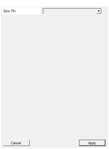
Set sync pin to use for this block
Which of the three R5560 / R5560SE SYNC LVDS lines this block reads. The choice determines the pin name, the pad name and the board signal.
| Value | Board signal | _P package pin |
|---|---|---|
SYNC_0 |
SYNC_0 |
C2 |
SYNC_1 |
SYNC_1 |
B2 |
SYNC_2 |
SYNC_2 |
A4 |
RedesignIfChanged is set - changing it rebuilds the symbol with a
differently named pin. It can be changed after the block is created.
Default: SYNC_0
Default: SYNC_0
Options: SYNC_0 SYNC_1 SYNC_2
⚙️ Detailed Operation
What the block compiles to
The pin name, the pad name and the source signal all follow the Sync Pin
property. For the default SYNC_0 the plug-in emits:
<your signal> <= SYNC_0;
plus one informational line in the compiler output:
Generating HDL code for <designator>
No process, no generic, no register map entry, no SciSDK endpoint.
The board side
The three sources are 1-bit vectors declared in the board’s top-level
template and driven by three IBUFDS primitives with on-die differential
termination enabled:
signal SYNC_0 : std_logic_vector(0 downto 0);
...
Besync_0_in : IBUFDS
generic map ( DIFF_TERM => TRUE, IBUF_LOW_PWR => FALSE, IOSTANDARD => "DEFAULT")
port map ( O => SYNC_0(0), I => SYNC_0_P, IB => SYNC_0_N );
with the constraints:
| Sync Pin | Board signal | Top-level ports | _P package pin |
I/O standard |
|---|---|---|---|---|
SYNC_0 |
SYNC_0 |
SYNC_0_P / SYNC_0_N |
C2 | LVDS |
SYNC_1 |
SYNC_1 |
SYNC_1_P / SYNC_1_N |
B2 | LVDS |
SYNC_2 |
SYNC_2 |
SYNC_2_P / SYNC_2_N |
A4 | LVDS |
The IBUFDS instances are present in every FPGA variant of both boards,
including the MINIMAL ones - unlike H-LINK, this block does
not quietly stop working on a reduced build.
Timing
Zero latency through the block itself; no clock, no reset, no debouncing and no enforced minimum pulse width. A pulse narrower than one clock period may be missed entirely by the synchroniser you add downstream.
Typical use
- Common start / common stop distributed over LVDS to a crate of boards.
- External trigger or gate from a master timing unit.
- Run / arm / veto level from a experiment-wide controller.
Board availability
SupportedBoard is GUID_BASED, and SupportedBoardGuids names two boards:
| Board GUID | Board plug-in |
|---|---|
F417C046-3AA0-4E63-964A-2008A6D35172 |
R5560 (boards/ni/board_R5560/bR5560.vb) |
C75E5DBB-6827-46A2-88BB-DBF38A36AAD7 |
R5560SE (boards/ni/board_R5560SE/bR5560SE.vb) |
The block is not offered on any other board, and no other board plug-in
declares a plain SYNC_n signal for it to read. On the DT5560 - a different
board GUID and a different signal naming - use Sync In /
Sync Out instead.
Unlike the DT5550-family board pins, this block is flagged as available inside sub-designs and inside state machines.