
Single Clock Delay
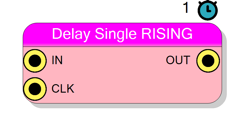
Single-cycle register delay element. Delays input signal by exactly one clock cycle with configurable edge sensitivity (rising or falling). Synchronous reset clears the register to zero. Latency: 1 clock cycle. Supports bit widths from 1 to 2048.
Introduction
This block implements a simple D-type register (flip-flop) that delays the input signal by exactly one clock cycle. It is the fundamental building block for creating pipeline stages and synchronization in digital designs.
The output updates on the selected clock edge (rising or falling):
$$ \mathrm{OUT}(n) = \mathrm{IN}(n-1), $$
where $n$ represents the current clock cycle. A synchronous reset forces the output to zero immediately.
Pin Description
Properties
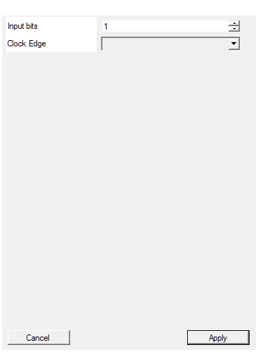
Set the number of bits of the input
Number of bits to delay. Range: 1 – 2048. Each bit requires one flip-flop in the FPGA fabric.Default: 1
Range: 1 – 2048
Select between rising and falling edge
Clock edge sensitivity. RISING: output updates on rising edge. FALLING: output updates on falling edge. Default: RISING.Default: RISING
Options: RISING FALLING
Functional description
The component implements a clocked register in VHDL that captures the input value on the active clock edge and presents it on the output.
Operation modes
The block supports two clock edge configurations:
- RISING edge: Output updates on rising edge of CLK (0 → 1 transition)
- FALLING edge: Output updates on falling edge of CLK (1 → 0 transition)
Reset behavior
The synchronous reset is active high:
- When RESET = 1, output is forced to all zeros.
- Reset takes effect on the next active clock edge.
Timing diagram
Example showing rising edge mode with 4-bit data:
Note: Output is delayed by exactly 1 clock cycle. After reset, output is 0.
Mathematical background
The single-cycle delay is equivalent to the z inverse operator in discrete-time signal processing (z-transform):
$$ Y(z) = z^{-1} \cdot X(z) $$
This represents a unit delay in the time domain: y[n] = x[n-1]
Timing
Fixed latency: 1 clock cycle
All TM phases have identical, deterministic latency.
Typical use cases
- Pipeline stages: Breaking long combinational paths to improve timing
- Synchronization: Aligning signals from different clock domains (with caution)
- Delay matching: Compensating for processing delays in parallel paths
- Data buffering: Simple FIFO elements in streaming applications
- Register insertion: Meeting timing constraints in high-speed designs