Getting Started with DT1260 (SciDK)
Step-by-step guide to create your first firmware project for the DT1260 (SciDK) board. This tutorial walks through creating a dual-channel waveform recorder with adjustable offset, compiling, programming the hardware, and testing with Resource Explorer.
Introduction
This chapter presents a step-by-step procedure to program the DT1260 (also called SciDK) board using SCI-Compiler. Additional examples are available as diagrams in the Example Project folder of SCI-Compiler for further exploration and customization.
What You’ll Build
In this tutorial, you will create firmware implementing:
- Dual-channel waveform recording on both analog inputs
- Adjustable signal offset via programmable DAC
- Oscilloscope readout for real-time waveform visualization
Prerequisites
Before starting, ensure you have:
- ✓ SCI-Compiler installed and licensed
- ✓ DT1260 hardware connected via USB
- ✓ USB drivers installed (automatic with SCI-Compiler)
- ✓ Xilinx Vivado 2017.4 installed (for local compilation)
Note: This tutorial follows the preliminary setup described in the Installation chapter.
Step 1: Launch SCI-Compiler
Open the SCI-Compiler application from your Windows Start menu or desktop shortcut.
Step 2: Create a New Project
- Click New Project in the toolbar or go to File → New Project
- Select SciDK-DT1260 as the target platform
- Choose a name for your project (e.g.,
MyFirstDT1260) - Select a folder location to save the project
- Press Create
A blank diagram page will open, ready for your design.
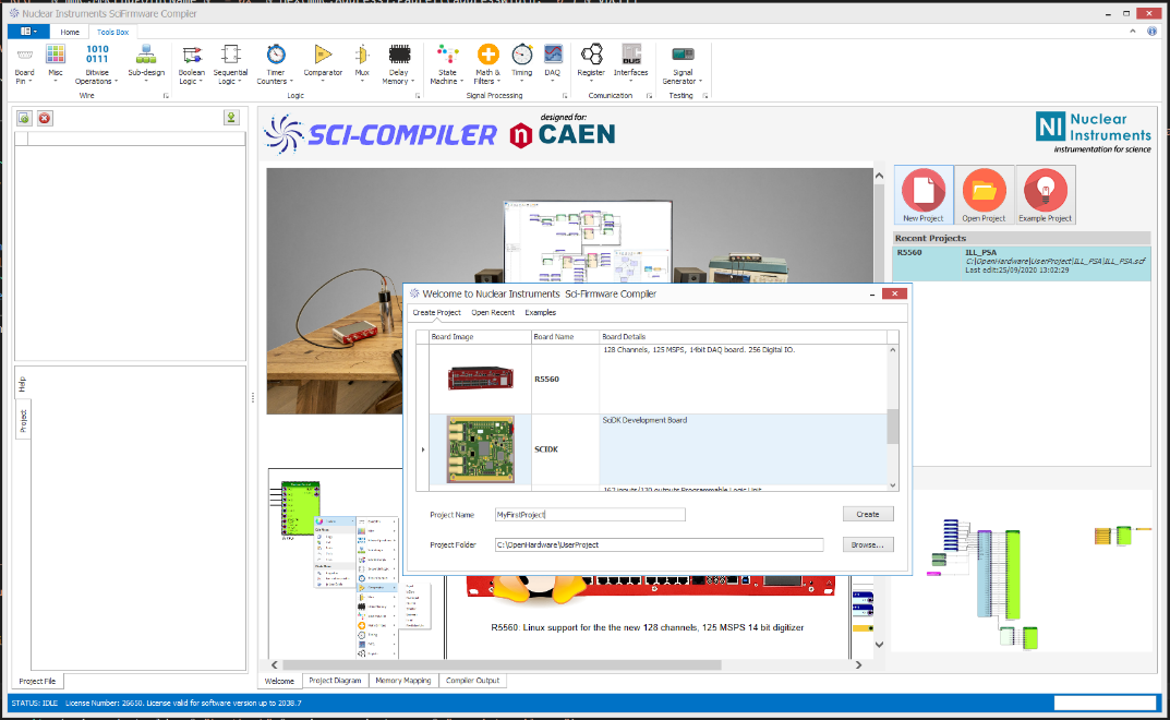
Figure 1: Creating a new project for DT1260 in SCI-Compiler
Step 3: Add Analog Input Blocks
The DT1260 has two analog input channels. We’ll add both to the design.
Add the Input Blocks
- From the top toolbar, select Board Pin → Analog In
- A selection window will open showing available analog inputs
- Select both rows (Channel 0 and Channel 1)
- Press OK
Two analog input blocks will appear on the diagram, representing the DT1260’s physical inputs.
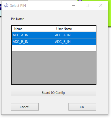
Figure 2: Selecting both analog input channels
Step 4: Add Oscilloscope Block
Now add a readout endpoint to capture and view the waveforms.
Add the Oscilloscope
- From the top toolbar, select DAQ → Oscilloscope
- The Oscilloscope block will be placed on the diagram
Configure the Oscilloscope
- Right-click on the Oscilloscope block
- Select Properties or Configure
- Set the parameters as shown below:
- Number of samples: 1024
- Number of channels: 2
- Data width: 12 (matches DT1260 ADC resolution)
- Analog Inputs: 2
- Digital Inputs: 0
- Press Apply
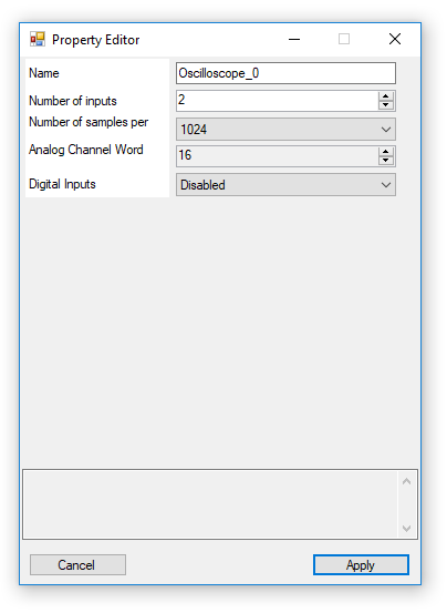
Figure 3: Configuring Oscilloscope parameters
Step 5: Connect the Blocks
Now connect the analog inputs to the oscilloscope.
Make the Connections
- Click on the output port of the first Analog In block (Channel 0)
- Drag to the first analog input of the Oscilloscope block
- Repeat for the second Analog In block (Channel 1)
Your diagram should now look like this:
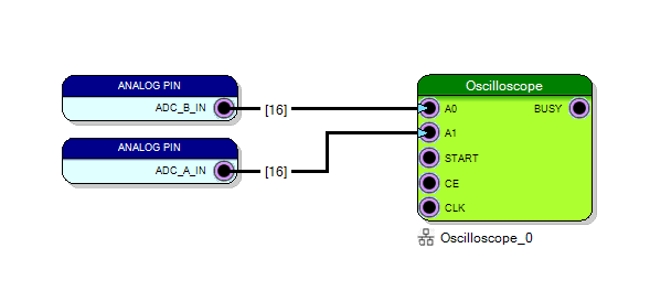
Figure 4: Connected block diagram
Connection summary:
- Analog In CH0 → Oscilloscope Analog Input 0
- Analog In CH1 → Oscilloscope Analog Input 1
Step 6: Assign Memory Mapping
Before compilation, we need to assign memory addresses to the Oscilloscope endpoint.
Configure Memory Map
- Go to the Memory Mapping tab (bottom of the screen)
- Press Refresh to detect all endpoints
- Press Auto Assign to automatically allocate memory addresses
The Oscilloscope and ANALOG_OFFSET register will be assigned addresses.
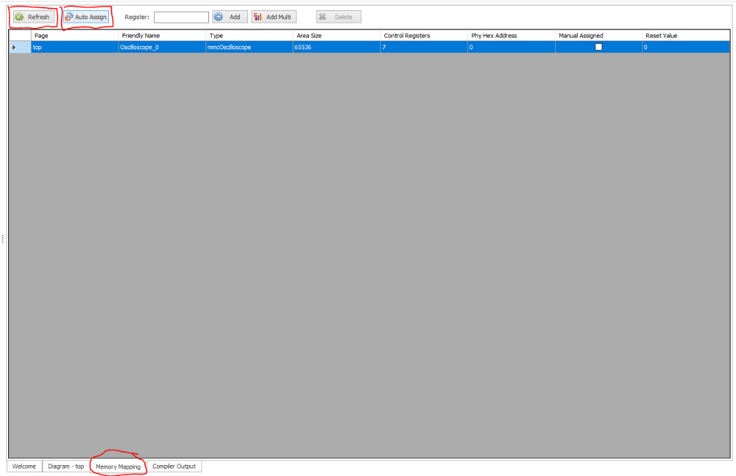
Figure 5: Memory mapping configuration
Step 7: Compile the Firmware
Now we’re ready to generate the FPGA firmware.
Start Compilation
- In the top toolbar, go to Home → Compile
- The compilation process will begin

Figure 6: Compile button in toolbar
Monitor Compilation Progress
- Watch the Compiler Output window for progress messages
- Compilation typically takes 10-20 minutes for DT1260
- Successful compilation shows “Compilation completed successfully”
Troubleshooting:
- If errors occur, check that all blocks are connected
- Verify memory mapping was completed
- Ensure Vivado 2017.4 is properly installed
Step 8: Generate Flash File
After successful compilation, generate the firmware file for programming.
Create Firmware File
- Click on Generate Flash File in the toolbar
- A
.niufirmware file will be created and saved in your project folder

Figure 7: Generate Flash File button
The firmware is now ready to be programmed into the DT1260.
Step 9: Enter Bootloader Mode
To program the DT1260, it must be in bootloader mode.
Switch to Bootloader
- Disconnect the DT1260 from USB
- Locate the bootloader switch on the rear panel
- Move the switch to the right (bootloader position)
- Reconnect the USB cable
The BL LED on the front panel should stay ON in blue (solid, not blinking).
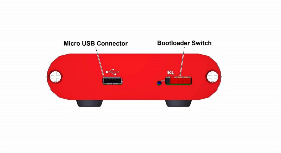
Figure 8: Bootloader switch position (right = bootloader mode)
Important: The blue LED must be solid ON. If it’s blinking, the board is in normal mode, not bootloader.
Step 10: Program the Firmware
Now use SCI-Compiler’s Flash Programming Tool to upload the firmware.
Launch Flash Tool
- From SCI-Compiler toolbar, press Flash Program Tool

Figure 9: Flash Program Tool button
Select Device
- The Flash Programming wizard will open
- Select SciDK-DT1260 from the dropdown menu
- Press Next
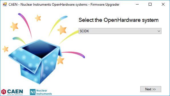
Figure 10: Select device type
Select Board PID
- Select the PID (Product ID) of your connected DT1260
- If no PID appears:
- Check USB connection
- Verify bootloader switch is in the right position
- Ensure USB drivers are installed
- Press Next
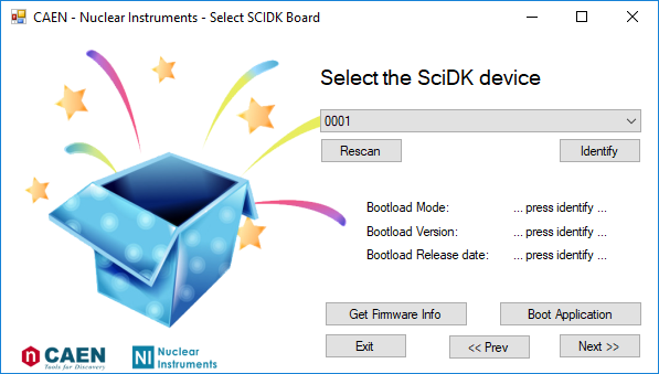
Figure 11: Select board PID
Browse and Program
- Click Browse and navigate to the
.niufirmware file in your project folder - Press Start to begin programming
- Wait for the process to complete (typically 30-60 seconds)
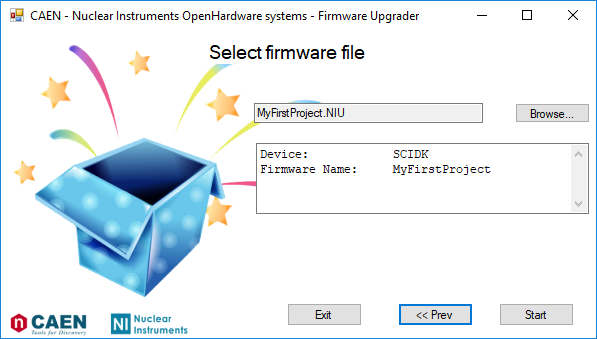
Figure 12: Select firmware file and start programming
Programming Complete
When finished, a success message will appear.
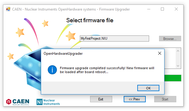
Figure 13: Firmware programming completed
Press OK to close the dialog.
Step 11: Switch to Normal Operation
After programming, return the board to normal operating mode.
Exit Bootloader Mode
- Disconnect the DT1260 from USB (power OFF)
- Move the bootloader switch to the left (normal operation)
- Reconnect the USB cable
After a few seconds, the BL LED should start blinking in blue, indicating the board is running valid firmware.
Success indicator: Blinking blue LED = firmware running correctly
Step 12: Open Resource Explorer
Now test the firmware using SCI-Compiler’s Resource Explorer tool.
Launch Resource Explorer
From SCI-Compiler toolbar, click Resource Explorer

Figure 14: Resource Explorer button
Step 13: Connect to the Board
Connect Resource Explorer to your DT1260 hardware.
Establish Connection
- Verify the DT1260 is connected via USB
- Select DT1260 from the model dropdown
- Choose the correct Serial Number / PID from the list
- Press Connect
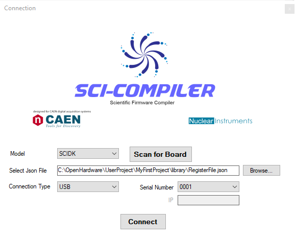
Figure 15: Connecting to DT1260 in Resource Explorer
Step 14: View Oscilloscope Data
Resource Explorer will enumerate all available endpoints in your firmware.
Open Oscilloscope Viewer
- In the Resource Explorer tree, you’ll see Oscilloscope_0 listed
- Right-click on Oscilloscope_0
- Select View
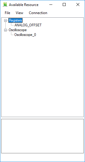
Figure 16: Opening Oscilloscope viewer
Step 15: Configure and Run Oscilloscope
Now configure the oscilloscope to capture waveforms.
Set Oscilloscope Parameters
Configure the following settings:
- Trigger Source: Free running (no external trigger needed)
- Trigger Mode: Auto
- Pretrigger: 0 (or desired value)
- Decimator: 1 (no decimation)
Press Play (▶ button) to start acquisition.
View Baseline
You should see two traces representing the baseline of both analog input channels:
- Blue trace: Channel 0
- Green trace: Channel 1
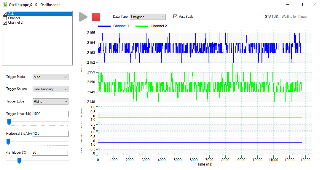
Figure 17: Oscilloscope displaying baseline traces
Note: The baseline appears at approximately mid-scale (~2048 counts) by default.
Step 16: Adjust Input Offset
Now test the ANALOG_OFFSET register to shift the input baseline.
Access the Offset Register
- In the Resource Explorer tree, locate ANALOG_OFFSET under Registers
- Right-click on ANALOG_OFFSET
- Select Set/Get
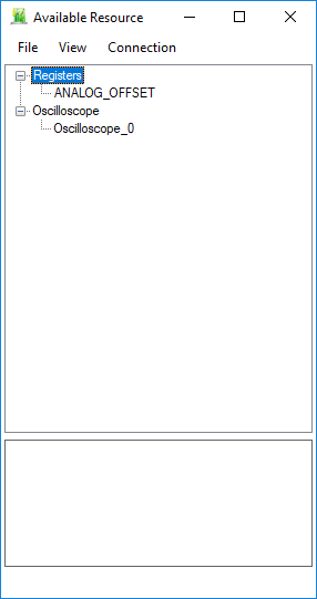
Figure 18: Accessing ANALOG_OFFSET register
Set a New Offset Value
- A register control dialog will appear
- Select Decimal mode
- Enter the value 1000
- Press Set
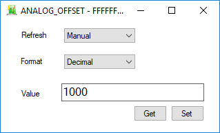
Figure 19: Setting offset to 1000
Observe the Result
After pressing Set, the oscilloscope traces will shift to approximately 1000 ADC counts.
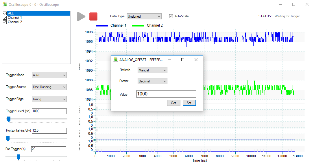
Figure 20: Baseline shifted to ~1000 counts after offset adjustment
What happened:
- The 12-bit DAC adjusted the analog offset
- Both input channels shifted by ~1000 counts
- This demonstrates real-time register control from Resource Explorer
Understanding the Results
Input Dynamic Range
The DT1260 has a 2 Vpp input range with 12-bit resolution (4096 levels):
| Input Voltage | ADC Value | Description |
|---|---|---|
| -1V | 0 | Minimum |
| 0V | ~2048 | Mid-scale (default) |
| +1V | 4095 | Maximum |
Offset Register Function
The ANALOG_OFFSET register controls a 12-bit DAC that adjusts the DC offset:
- Value 0: Baseline at ~0 (maximum negative offset)
- Value 2048: Baseline at ~2048 (centered, default)
- Value 4095: Baseline at ~4095 (maximum positive offset)
Use cases:
- Positive signals only: Set offset to 0 to use full dynamic range
- Negative signals only: Set offset to 4095
- Bipolar signals: Set offset to 2048 for symmetric coverage
Next Steps
Congratulations! You’ve successfully:
- ✓ Created a firmware design in SCI-Compiler
- ✓ Compiled FPGA firmware
- ✓ Programmed the DT1260 hardware
- ✓ Tested with Resource Explorer
- ✓ Controlled registers in real-time
Experiment Further
Try these modifications to learn more:
-
Add a signal source:
- Connect a function generator to Channel 0 input
- Set trigger to “Analog Input 0”
- Adjust threshold to capture pulses
-
Add more processing:
- Insert a Trigger Discriminator block
- Add a Baseline Restorer
- Experiment with Digital Shapers
-
Add a Spectrum endpoint:
- Include a Spectrum block for MCA functionality
- Connect energy values from shapers
- View histogram in Resource Explorer
-
Use digital I/O:
- Add Digital Out blocks
- Generate trigger output signals
- Create gate patterns
Advanced Topics
Once comfortable with the basics, explore:
- Trapezoidal filters for energy measurement
- Time-of-Flight (ToF) measurements
- Custom trigger logic
- List mode for event-by-event data
- Software integration with SciSDK (Python, C++)
Troubleshooting
Compilation Fails
Problem: Vivado reports errors during compilation
Solutions:
- Verify all blocks are properly connected
- Check that memory mapping was completed
- Ensure Vivado 2017.4 is correctly installed
- Review error messages in Compiler Output window
Flash Programming Fails
Problem: Flash tool cannot find the device
Solutions:
- Check bootloader switch is in the right position
- Verify USB cable connection
- Ensure BL LED is solid blue (not blinking)
- Try a different USB port (avoid hubs)
- Reinstall USB drivers from SCI-Compiler
No Signal in Resource Explorer
Problem: Oscilloscope shows flat line or no data
Solutions:
- Verify board is in normal mode (bootloader switch left)
- Check BL LED is blinking blue (firmware running)
- Select “Free running” trigger mode for baseline view
- Ensure correct board PID is selected in Resource Explorer
Baseline Not Shifting with Offset
Problem: ANALOG_OFFSET register has no effect
Solutions:
- Verify the register appears in memory mapping
- Check value is in range 0-4095
- Allow 100ms for DAC to settle
- Re-read offset value to verify it was set
Summary
This tutorial covered the complete workflow for DT1260 firmware development:
| Step | Action | Tool |
|---|---|---|
| Design | Create block diagram | SCI-Compiler Editor |
| Compile | Generate VHDL and bitstream | Xilinx Vivado |
| Program | Upload firmware to flash | Flash Program Tool |
| Test | View data and control registers | Resource Explorer |
You now have the foundation to create more complex designs. Experiment with the example projects included with SCI-Compiler and explore the extensive block library to build custom signal processing systems.
Happy FPGA programming!