
Voltage Regulator
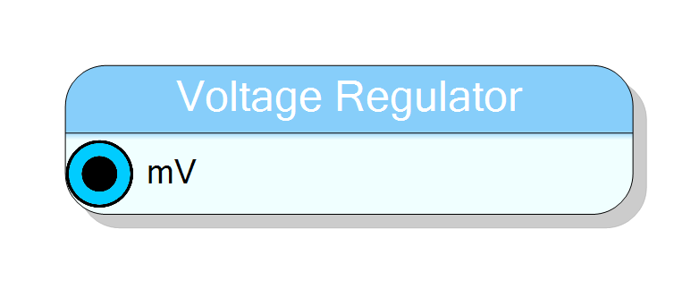
Board pin block that sets the programmable supply voltage of one of the two DT5550 Digital I/O connectors. The 16-bit input is a plain millivolt number; it is not driven to a DAC by the FPGA but published in the FPGA’s on-board I2C slave register, from where the board system controller reads it and programs the regulator. No logic, no register, no software-visible endpoint.
Introduction
Principle of Operation
Voltage Regulator is a Board Pin block: it is not a piece of logic, it is the diagram-side handle on a piece of board hardware - the programmable supply that powers one of the two Digital I/O connectors of the DT5550.
Placing the block lets your design choose that voltage at run time. The
16-bit value you wire into mV is interpreted as a voltage in
millivolts (e.g. 3300 = 3.3 V).
The path is indirect, and knowing that matters when you debug it:
your logic ──16──► POWER_SUPPLY_OUTn_mV ──► sys_controller_iic_slave
│ (FPGA is the I2C SLAVE,
│ 7-bit address 0000100b)
▼
board system controller (MCU)
│
▼
Digital I/O connector supply
The FPGA never drives the regulator directly. It only advertises the requested voltage in a register the board controller polls over the system I2C bus. Nothing in the FPGA fabric changes when you change the value - the change happens when the controller next reads the register.
Pin Description
Requested output voltage, in millivolts (canvas caption mV).
Plain unsigned 16-bit number: 3300 means 3.3 V.
Sampled once per I2C read transaction by the board system controller, not every clock - hold it stable.
There is no open guard on this pad: the assignment is emitted
unconditionally, so wire it. If you leave it open the block has
nothing to contribute and the connector keeps the template default
(3300 mV on A, 2500 mV on B).
Properties
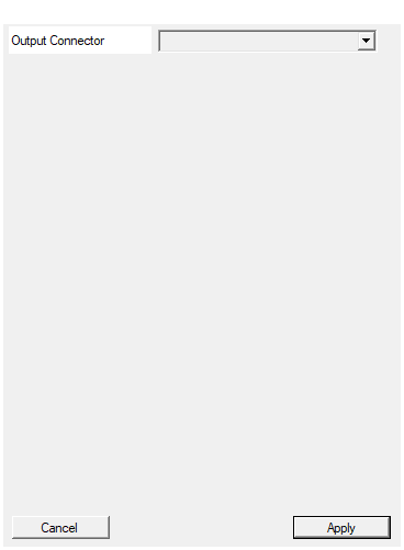
Select the output connector for the voltage regulator
Which of the two DT5550 Digital I/O connectors this block programs. Selecting the connector selects the target board signal, and therefore which half of the I2C register the value lands in.
| Value | Board signal | I2C register bits | Template default |
|---|---|---|---|
DIGITAL I/O A |
POWER_SUPPLY_OUT1_mV |
15:0 | x"0CE4" = 3300 mV |
DIGITAL I/O B |
POWER_SUPPLY_OUT2_mV |
31:16 | x"09C4" = 2500 mV |
RedesignIfChanged is set, so the symbol is rebuilt when you change it
(the pin list itself does not change). It can be changed after the block
is created.
Default: DIGITAL I/O A
Default: DIGITAL I/O A
Options: DIGITAL I/O A DIGITAL I/O B
⚙️ Detailed Operation
What the block compiles to
CompileHDL adds one 16-bit input pad V and emits a single concurrent
assignment. Which board signal is targeted depends on the
Output Connector property:
| Output Connector | Emitted line |
|---|---|
DIGITAL I/O A |
POWER_SUPPLY_OUT1_mV <= <your signal>; |
DIGITAL I/O B |
POWER_SUPPLY_OUT2_mV <= <your signal>; |
That is the whole block. No process, no flip-flop, no generic, no compiler message.
The board side
Both targets are 16-bit signals declared by the DT5550 top-level template
(dt5550b_top.vht) with a default value:
signal POWER_SUPPLY_OUT1_mV : std_logic_Vector(15 downto 0) := x"0CE4"; -- 3300 mV
signal POWER_SUPPLY_OUT2_mV : std_logic_Vector(15 downto 0) := x"09C4"; -- 2500 mV
So a design without this block still has a defined supply voltage: 3300 mV on Digital I/O A and 2500 mV on Digital I/O B. Placing the block replaces the default with your value (a concurrent driver wins over an initial value from time zero onwards).
Both signals go straight into the sys_controller_iic_slave instance:
SyPWR : sys_controller_iic_slave
Port MAP( clk => CLK_80(0),
reset => '0',
iic_sda => sys_iic_sda,
iic_scl => sys_iic_scl,
mVout1 => POWER_SUPPLY_OUT1_mV,
mVout2 => POWER_SUPPLY_OUT2_mV );
Inside that slave the two words are simply concatenated into the 32-bit read register
vhdl
reg_data_rd <= mVout2 & mVout1;
i.e. Digital I/O A in bits 15:0, Digital I/O B in bits 31:16. The I2C
core answers at 7-bit slave address 0000100 and the command decoder
latches the whole 32-bit word once, at the start of a read transfer
(int_reg_data <= reg_data_rd on the phy_start / read edge), then shifts
it out byte by byte. The register is clocked by CLK_80(0).
Timing
There is no defined latency for this block in the useful sense: the fabric side is combinational (zero clocks), but the moment the physical supply actually moves is set by how often the board controller polls the register and how fast the regulator slews. Neither is visible from the firmware and neither is specified here.
Because the value is sampled once per I2C transaction, drive mV from a
register or a constant, not from something that changes every clock - a
value that moves while the controller is mid-transaction is simply the value
that happened to be there at phy_start.
Typical use
- Matching the Digital I/O connector level to whatever is plugged into it (for example 3.3 V vs 2.5 V logic) from a constant in the diagram.
- Letting a register written by software select the level, by driving mV from a software-visible register block.
Board availability
This block is offered only on the DT5550 (board plug-in GUID
413F904B-7FD0-43EF-B127-74278C23F1A5).
The class also lists DT5550SE and DT5560 in SupportedBoard, but that has
no effect:
- the toolbox visibility filter (
Form1_plugins.vb) implements a branch forBOARD_MODELS.DT5550only - there is noDT5550SEorDT5560branch; - no board plug-in in the repository declares itself as
DT5550SE; - the DT5560 top-level template declares no
POWER_SUPPLY_OUT*_mVsignal at all, so even if the block were placed there the generated VHDL would reference an undeclared signal.