
FFT Filter TM Prog
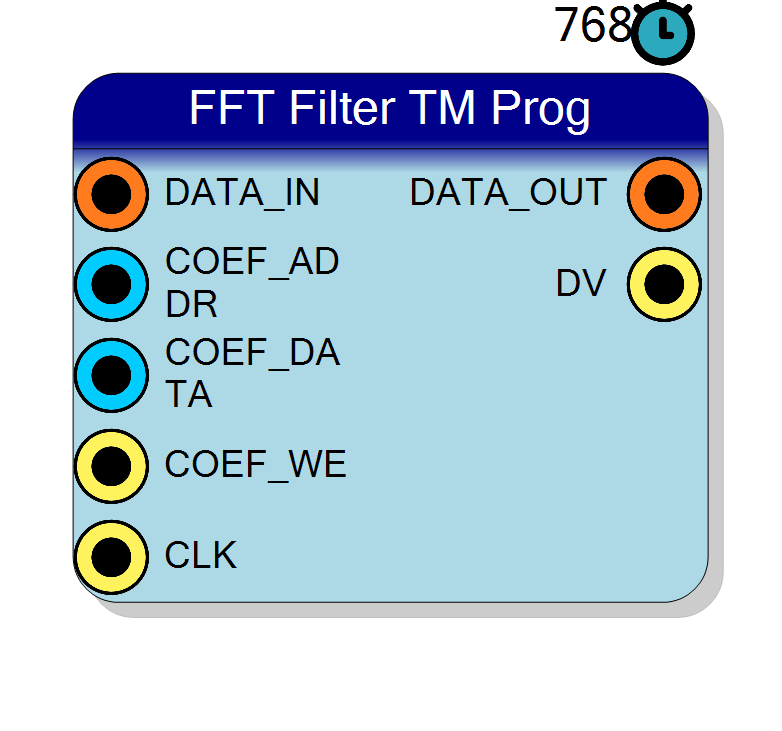
Runtime-programmable variant of FFT Filter TM: the same full-rate overlap-save fast-convolution engine (two forward and two inverse polyphase FFT chains, 4R xfft cores of N/R points) but the frequency response H[k] lives in RAM and is written at run time through a COEF_ADDR / COEF_DATA / COEF_WE bus. Unity passthrough until loaded. No custom GUI - only FFT length and TM factor are set at compile time.
Introduction
Principle of Operation
This block is FFT Filter TM with a writable frequency response. The
datapath is emitted by the same generator
(Component_FFTFilterTM.SharedCompileHDL, called with programmable = True),
so the filtering principle is identical: a TM stream of $R$ samples per clock is
convolved with an impulse response of up to $N/2$ taps by multiplying its
spectrum, using 50 % overlap-save so that the output is continuous and in order.
$$ y[n] ;=; \mathcal{F}^{-1}\big{,H[k]\cdot X[k],\big} $$
The only difference from the fixed block is where $H[k]$ comes from:
| FFT Filter TM | FFT Filter TM Prog | |
|---|---|---|
| $H[k]$ storage | VHDL constant ROM (HRE_q, HIM_q) |
VHDL signal RAM |
| Set by | the FFT Filter designer (double-click) | the COEF_* bus, at run time |
| Value before load | the designed response | HRE = 0x7FFF, HIM = 0x0000 → unity passthrough |
| Extra pins | – | COEF_ADDR, COEF_DATA, COEF_WE |
| Properties | Length, TMFactor, Filter, FFProject | Length, TMFactor |
Use it when the filter must change without re-running synthesis: an operator- selected band, an adaptive notch, a response computed on the host and pushed down, or one design reused for several detector configurations.
To design a response, place a fixed FFT Filter TM block and use its designer (LP/HP/BP/BS presets, hand-drawn response, coefficients from file); its H[k] CSV export produces exactly the address map this block expects.
Pin Description
ceil(log2 N) + 1 bits.
0 … N-1 writes H_RE[k], N … 2N-1 writes H_IM[k-N].
The polyphase lane and index are derived inside the wrapper.
0x7FFF = +0.99997, 0x4000 = +0.5,
0x0000 = 0, 0x8000 = -1.0. Values are clamped to the signed 16-bit
range when they come from the designer.
COEF_DATA at COEF_ADDR.
No frame-boundary interlock: the new coefficient is used from the next bin.
DATA_IN, in order.
Properties
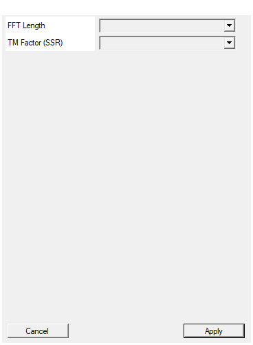
FFT block size N (power of 2). Filter impulse response up to N/2 taps.
FFT block size $N$, a power of two. Available values: 256, 512, 1024, 2048, 4096, 8192, 16384. The impulse response may be up to $N/2$ taps long (50 % overlap-save), and each of the4 x TMFactor instantiated xfft cores is $N/\text{TMFactor}$
points.
Default: 1024
Default: 1024
Options: 256 512 1024 2048 4096 8192 16384
Time Multiplexing factor (samples per clock). 2 or 4.
Time-multiplexing factor $R$ = samples per clock onDATA_IN and
DATA_OUT.
Available values: 2, 4 — nothing else compiles.
Default: 4
Default: 4
Options: 2 4
⚙️ Loading H[k]
One coefficient per clock, on a plain synchronous write port:
COEF_ADDR <= a -- see the address map below
COEF_DATA <= h -- signed Q15, 0x7FFF = +0.99997, 0x8000 = -1.0
COEF_WE <= '1' -- one clock
COEF_ADDR is ceil(log2 N) + 1 bits wide — one bit more than the bin index —
because the real and the imaginary tables share one address space:
| Address range | Written table |
|---|---|
0 … N-1 |
H_RE[k], bin k = address |
N … 2N-1 |
H_IM[k], bin k = address - N |
Internally the top bit selects RE vs IM and the bin index is split across the polyphase banks, which you do not have to do yourself:
$$ \text{lane } q = \left\lfloor k / M \right\rfloor, \qquad \text{index} = k \bmod M, \qquad M = N/R $$
Writing addresses 0 … 2N-1 in natural order therefore loads the whole
response.
Until the first write the RAMs hold HRE_q = 0x7FFF, HIM_q = 0x0000 in every
cell, i.e. $H[k] \approx 1$ for all $k$: the block is a unity passthrough
(with the pipeline latency of the full FFT/IFFT chain).
The engine, in one picture
+-- fwd polyphase FFT --+ x H[k] (Q15, per lane) +-- inv polyphase FFT --+
DATA_IN (R/clk) --+-| engine A |------------------------->| Scale | --+
| +-----------------------+ +-----------------------+ |
| delay |
| M/2 clk |
| +-----------------------+ +-----------------------+ +--> keep 2nd half
+-| delay N/2 samples |-- fwd engine B ---------->| Scale | --+ of each frame
+-----------------------+ +-----------------------+ -> DATA_OUT
- Two forward chains. Engine A transforms frames $[jN,\ jN+N)$; engine B sees the input through a delay line of $N/2$ samples ($M/2$ clocks) so it covers the interleaved frames.
- Per-lane complex multiply. Lane $q$ holds bins $k + qM$; the multiply is
a 3-stage pipeline of four real products (
c1_rr,c1_ii,c1_ri,c1_ir) per lane and engine — $2R$ complex multipliers in total. - Two inverse chains, configured
Scale, bring the result back to 16 bit. - Overlap-save keep rule. Only the second half of every reconstructed
frame is valid (
keep := '1'when the output position within the frame is $\ge M/2$). Engine A’s kept half is re-timed by $M/2$ clocks (adlydelay line,Component_FFTFilterTM.vbaround theadly_tdeclaration) so that B’s half, A’s half, B’s next half tile exactly:DATA_OUTis continuous and in order, andDVstays high.
Note for maintainers: the class header comment says engine A is delayed by
M = N/Rclocks, but the wrapper the generator actually emits usesH2 = M \ 2for both the engine-B input delay line and the engine-A output delay line. The emitted VHDL is the behaviour; the header comment (and the older FFT Filter TM page) disagree with it.
Internal widths
With Length = $N$, TMFactor = $R$, $M = N/R$:
$$ XB ;=; \min!\big(16 + \lceil \log_2 N \rceil + 1,; 30\big) $$
is the unscaled forward-FFT output width per lane; the inverse core is instantiated with an input width of $XB + \lceil \log_2 R \rceil + 1$. The clamp at 30 bits is the inverse polyphase input cap, so for very large $N$ the forward result is truncated to 30 bits before the multiply.
Input and output are fixed at 16 bit per sample — unlike FFT Windowed TM
there is no InputBits property.
Generated hardware
CompileHDL writes into the project’s pcores/ folder:
xftmp_f_<designator>.tclandxftmp_i_<designator>.tcl— two Xilinx xfft IP configurations oftransform_length$M$,pipelined_streaming_io,phase_factor_width 16,scaling_options unscaled,rounding_modes convergent_rounding,output_ordering natural_order,aresetn true; the forward one withinput_width 16, the inverse one withinput_width = XB + log2(R) + 1;ssrf_fft_ftmp_<designator>.vhd/ssri_fft_ftmp_<designator>.vhd— the forward and inverse polyphase wrappers (shared with FFT TM Realtime / IFFT TM Realtime);fft_ftmp_<designator>.vhd— the top level: H RAMs, the load port, the delay lines, the multipliers and the keep/mux logic.
At compile time the log carries an informational line of the form
Generating FFT Filter TM for <designator> (N=1024, R=4, overlap-save 50%,
2x fwd + 2x inv polyphase engines = 16 xfft cores, programmable H)
The block is declared _ANY_XLX, i.e. Xilinx targets only.
Cost
- $4R$
xfftcores of $N/R$ points. For $R = 4$, $N = 1024$: 16 cores of 256 points. This is the price of full rate on a TM stream. - $2R$ complex multipliers (4 real products each) for the $H[k]$ stage.
- $2R$ RAM banks of $M \times 16$ bit for
HRE_q/HIM_q, plus two delay lines of $M/2$ words.
Constraints and failure modes
-
TMFactormust be 2 or 4. Anything else aborts the compile with<designator>: FFT Filter TM supports TM factor 2 or 4 only. Selected: <R> -
LengthandTMFactorboth haveRedesignIfChanged = True: changing either re-draws the symbol (theCOEF_ADDRwidth follows $N$) and re-generates the IP. -
Impulse responses longer than $N/2$ taps cannot be represented — that is the overlap-save limit, not a property check; pick a larger
Length. -
Not available inside a state machine (
AvailableInStateMachine = False); available in sub-designs. -
There is no
RESETpin on the symbol:resetis wired automatically to the project global reset, andclkdefaults to the project acquisition clock.
Resources & Timing
-
Latency: The symbol declares a latency of 3 * (N / TMFactor) clocks (bxs.Latency = 3 * (N \ R)) - forward FFT, multiply, inverse FFT plus the overlap-save re-timing. That is the figure the compiler uses for automatic delay matching; no cycle-exact figure is stated in the sources.
-
Throughput: Full rate: TMFactor samples in and TMFactor samples out every clock, DV continuous.
- Xilinx only (
SupportedBoard = _ANY_XLX). - 4 x TMFactor xfft cores of N/TMFactor points + 2 x TMFactor complex multipliers.
- Input and output are fixed at 16 bit per sample.
- Unity passthrough until H[k] is written.