
FFT Filter Prog
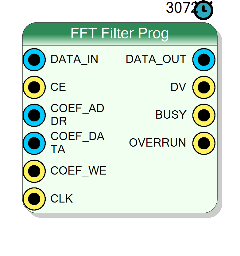
Runtime-programmable FFT-based filter (fast convolution, overlap-save 50%): same engine as FFT Filter but H[k] lives in RAM and is loaded through a COEF_ADDR / COEF_DATA / COEF_WE bus. Standard properties, no GUI - generate the coefficient file with the FFT Filter designer.
Introduction
See the FFT Filter guide for the datapath, operation (full rate up to CE duty 100%, latency ~2.5 N) and design notes. This variant starts as a passthrough (H = 1) and takes its complex Q15 response at runtime: write RE[k] at address k and IM[k] at address N+k (address bit log2(N) selects the part), one COEF_WE pulse per value. Load while the input is idle. The FFT Filter designer CSV export produces exactly this address map.
Pin Description
Properties
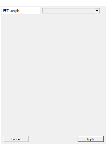
FFT block size N (power of 2). H[k] loaded via COEF bus: addr bit log2(N) selects RE(0)/IM(1), data Q15.
FFT block size N (256..16384).Default: 1024
Options: 256 512 1024 2048 4096 8192 16384