
Altera PLL
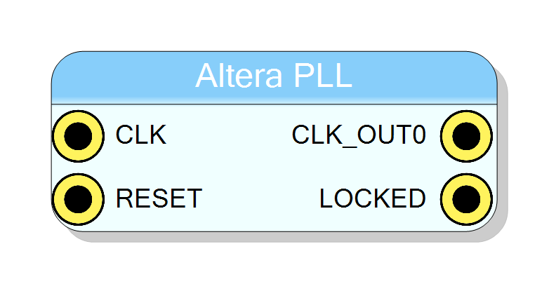
Instantiates an Intel/Altera FPGA PLL to generate custom clock frequencies. Supports up to 8 output clocks with configurable frequency and phase.
Introduction
The Altera PLL block instantiates one of the PLLs available in Intel/Altera FPGAs to generate custom clock frequencies in the range 10 MHz to 500 MHz.
The generated clocks can be used internally within the FPGA or distributed externally using standard I/O pins.
Pin Description
PLL lock indicator output.
- High (1): PLL is locked, output clocks are valid
- Low (0): PLL is not locked, output clocks are invalid Monitor with an LED to check for clock issues.
Properties
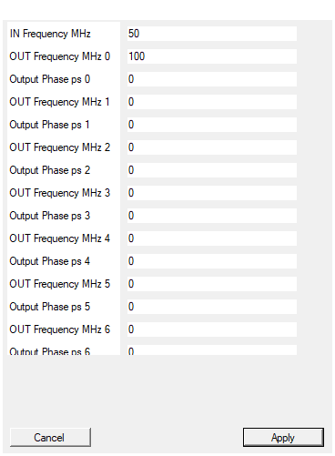
Set the value of provided input clock frequency.
Input clock frequency in MHz. Must match the actual frequency of the clock connected to the CLK input. Valid range: 10 - 500 MHz, default 50 MHz.Default: 50
Set the value of the clock frequency
Default: 100
Set the value of the clock frequency.
Default: 0
Set the value of the clock frequency
Default: 0
Set the value of the clock frequency.
Default: 0
Set the value of the clock frequency
Default: 0
Set the value of the clock frequency.
Default: 0
Set the value of the clock frequency
Default: 0
Set the value of the clock frequency.
Default: 0
Set the value of the clock frequency
Default: 0
Set the value of the clock frequency.
Default: 0
Set the value of the clock frequency
Default: 0
Set the value of the clock frequency.
Default: 0
Set the value of the clock frequency
Default: 0
Set the value of the clock frequency.
Default: 0
Set the value of the clock frequency
Default: 0
Set the value of the clock frequency.
Default: 0
Usage
PLL Architecture
The PLL (Phase-Locked Loop) in the FPGA is a mixed analog/digital circuit consisting of:
- VCO (Voltage Controlled Oscillator): Produces a high internal frequency (in the order of several GHz)
- Frequency Dividers: Each output is connected to the VCO through a programmable divider
- Phase Detectors: Compare input and feedback clocks to maintain lock
Input Clock Requirements
The input clock must meet the following specifications:
| Parameter | Requirement |
|---|---|
| Frequency Range | 10 - 500 MHz |
| Jitter | Less than 10 ps RMS |
| Duty Cycle | 50% |
| Source | Board clock or external I/O |
The input clock can be one of the available clocks on the board or any I/O input. It is mandatory to correctly configure the input clock frequency in the component properties.
Output Frequency Generation
The tool calculates a best-effort configuration to match all the frequencies requested by the user. Due to the nature of PLL dividers, it is not possible to know a priori the exact frequency that will be generated for each output.
To ensure accurate frequencies: Request only frequencies that are integer multiples of each other on a single PLL.
For example:
- Good: 50 MHz, 100 MHz, 200 MHz (all are multiples)
- Problematic: 50 MHz, 75 MHz, 100 MHz (75 is not a simple multiple)
Phase Configuration
It is possible to configure the phase relationship between different output clocks. The phase is specified as a delay in picoseconds (ps) relative to the input clock phase.
This is useful for:
- Creating clock domains with specific timing relationships
- DDR interfacing where 90-degree phase shifts are needed
- Compensating for routing delays
Output Channel Limitations
Important: It is not possible to enable a set of channels that are not contiguous. This is a limitation of the PLL hardware in the FPGA.
For example, if you need 3 clock outputs:
- Valid: Outputs 0, 1, 2
- Invalid: Outputs 0, 1, 3 (will trigger a compilation error)
To disable a clock output, set its frequency to 0. The symbol in SciCompiler will automatically adapt to show only the enabled clock outputs.
Lock Indicator
The LOCKED output indicates when the PLL internal loop is locked and valid clock outputs are being generated. Monitor this signal (e.g., with an LED) to detect clock issues.
Conditions that may cause loss of lock:
- Incorrect input clock frequency setting
- Noisy input clock
- Non-symmetrical (non-50% duty cycle) input clock
- Input frequency outside valid range