
RF CIC Interpolator (programmable rate)
Cascaded-Integrator-Comb (CIC) interpolator for a complex I/Q baseband stream whose interpolation factor R is a run-time input pin (RATE) rather than a compile-time constant. The accumulator is sized for a worst-case MaxRate, letting the fabric retune the up-sampling ratio on the fly - ideal for a software-defined DUC whose output rate must track a selected DAC configuration.
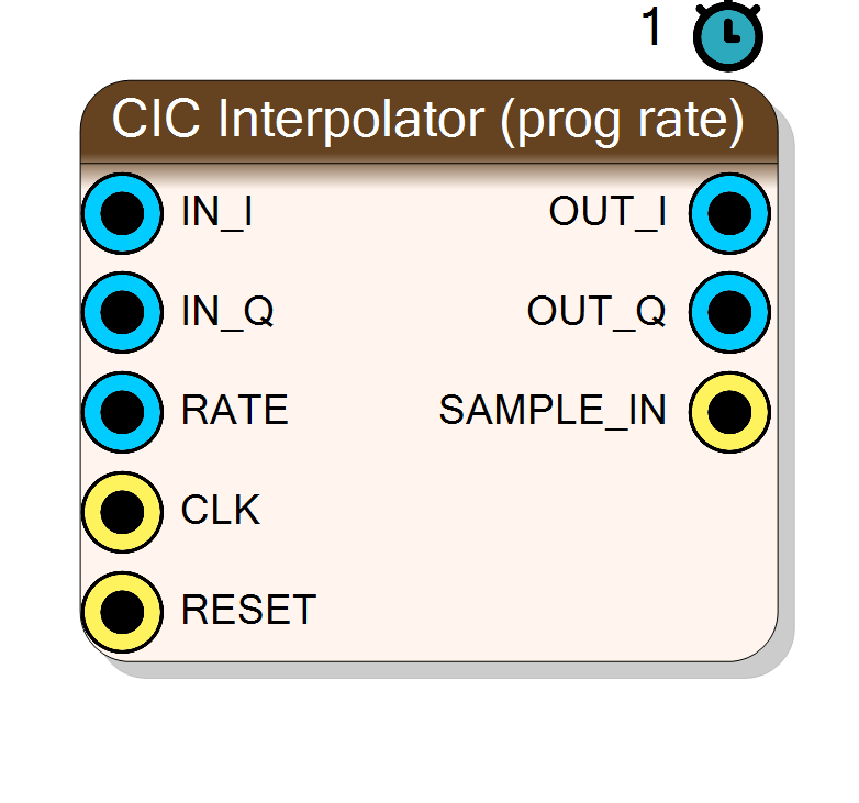
Introduction
The CIC Interpolator (programmable rate) is the same multiplier-free
cascaded-integrator-comb core as Component_CICInterpolator (it shares
the identical HLS source, cic_interp.cpp, and top function cic_interp),
but the interpolation ratio R is driven by a top-level RATE input
bus instead of being baked in. The fabric can change R at any time; the
change takes effect at the next rate-counter rollover.
x[m] ─► [ N combs @ Fs_out/R ] ─► ( ↑R ) ─► [ N integrators @ Fs_out ] ─► y[n]
▲
RATE pin (1..MaxRate)
The block runs at the fast output rate Fs_out; the effective low input
rate is Fs_in = Fs_out / R. The transfer function and sinc^N magnitude
response are exactly as in the fixed-rate block:
H(z) = [ (1 - z^-(R*M)) / (1 - z^-1) ]^N
|H(f)| = | sin(pi*R*M*f/Fs_out) / sin(pi*f/Fs_out) |^N
Because R is unknown at synthesis time, the datapath is sized for the largest rate you intend to use (the MaxRate property), so it is wider than a fixed-rate block of the same nominal R.
See Component_CICInterpolator (cic_interp) for the full CIC
interpolation theory and the SAMPLE_IN handshake; this page focuses on
the run-time-rate specifics.
Pin Description
SAMPLE_IN strobe; hold stable until then.
2 .. MaxRate; a change takes effect at the next rate-counter
rollover.
Fs_out = R * Fs_in. Default: Acquisition clock.
In-phase (I) interpolated output at the fast rate. Signed, **InputSize
- Nceil(log2(MaxRateM))** bits. Valid on every clock; carries the
live
(R*M)^NDC gain.
Quadrature (Q) interpolated output at the fast rate. Signed, **InputSize
- Nceil(log2(MaxRateM))** bits. Valid on every clock.
R output
clocks (live R) on the cycle where the block consumes IN_I/IN_Q.
Use it to pace the upstream producer. Not an output-valid flag.
Properties
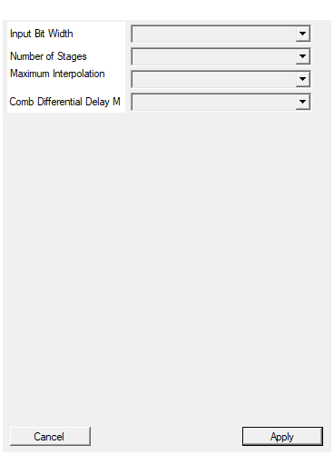
Bit width of each I/Q input sample (signed).
Bit width of each signed I / Q input sample. Range 4 to 32, default 16. Redesign on change.Default: 16
Options: 4 5 6 7 8 9 10 11 12 13 14 15 16 17 18 19 20 21 22 23 24 25 26 27 28 29 30 31 32
Filter order N.
Number of comb/integrator stages N (CIC order). Choices 1..6, default 3. Higher N deepens image rejection but addsceil(log2(MaxRate*M)) bits of growth per stage and more passband
droop. Redesign on change.
Default: 3
Options: 1 2 3 4 5 6
Upper bound on R. Sizes the accumulator and the RATE bus.
Upper bound on the run-time interpolation factor R. Sizes the accumulator width (InputSize + N*ceil(log2(MaxRate*M)) bits) and the
RATE bus width (ceil(log2(MaxRate)) + 1 bits). Pick the smallest
MaxRate that covers your range to save logic. Choices 4, 8, 16, 32,
64, 128, 256, 512, default 64. Redesign on change.
Default: 64
Options: 4 8 16 32 64 128 256 512
Differential delay (usually 1).
Comb differential delay M (low-rate samples). Almost always 1;M=2 widens the stop-band notches. Choices 1, 2, default 1.
Default: 1
Options: 1 2
Usage
The RATE pin
RATE is an unsigned bus carrying the current interpolation factor. Its
width is
RATE_SIZE = ceil(log2(MaxRate)) + 1 bits
The extra bit lets the value equal MaxRate itself. Drive RATE with a
value in 2 .. MaxRate; the block then consumes one low-rate input every R
output clocks and interpolates in between.
Worked example (default MaxRate = 64):
RATE_SIZE = ceil(log2(64)) + 1 = 7 bits (holds 0..64)
SAMPLE_IN handshake (input pacing)
Identical in meaning to the fixed-rate block: SAMPLE_IN is a
one-clock-wide input-request strobe asserted once every R output clocks
on the cycle the block consumes IN_I/IN_Q. Hold each low-rate input
stable until SAMPLE_IN, then advance the producer. Every output clock
carries a valid interpolated sample - there is no output-valid flag.
CLK _|‾|_|‾|_ ... (R output clocks) ... _|‾|_
SAMPLE_IN __|‾|____ ... consume x[m] ...__|‾|_
After a run-time rate change the internal comb/integrator state reflects the previous rate for a few samples; allow the filter to settle.
Bit growth is set by MaxRate
The accumulator width must survive the worst-case DC gain, so it is sized
from MaxRate, independent of the live RATE:
GROWTH = N * ceil(log2(MaxRate * M))
OUT_SIZE = INPUT_SIZE + GROWTH
DC gain = (R * M)^N (with the LIVE R, at run time)
Worked example (defaults N=3, MaxRate=64, M=1, InputSize=16):
GROWTH = 3 * ceil(log2(64)) = 18 bits
OUT_SIZE = 16 + 18 = 34 bits
RATE_SIZE = 7 bits
The DC gain on OUT_I/OUT_Q is (R*M)^N with the live R, so it changes
when you change the rate - account for this in any downstream scaling/AGC.
Timing, interface and reset
#pragma HLS PIPELINE II=1: one output sample pair per clock atFs_out.RATEuses theap_stableHLS interface; all other ports useap_none.RESET(ap_rst) clears comb delay lines, integrator accumulators and the rate counter.
Typical applications
- Software-defined DUC whose interpolation follows a host-selected baseband/DAC configuration without re-synthesising the bitstream.
- Multi-mode transmitters switching output rate between modes.
- Adaptive sample-rate matching between a variable DSP rate and a fixed converter clock.
Resources & Timing
-
Latency: Symbol/scheduling latency 1 clock; interpolated stream valid every output clock. Group delay ~NRM/2 output samples. Allow settling after a run-time rate change.
-
Throughput: 1 output sample pair per clock (II=1) at Fs_out; one low-rate input consumed every R output clocks (live R), paced by SAMPLE_IN.
Same HLS core as the fixed-rate cic_interp (top function cic_interp),
with RATE promoted to a top-level ap_stable port. Datapath sized for
MaxRate, so wider/costlier than a fixed-rate block of equal nominal R -
use the smallest MaxRate you need. Multiplier-free: 2N comb subtractors +
2N integrator adders + one counter. Output carries the live (R*M)^N
gain; scale downstream and pre-compensate droop with an interpolation FIR
before the CIC.