
D Flip-Flop (Rising Edge)
Rising-edge-triggered D-type flip-flop for reliable synchronous data storage. Samples multi-bit input data on rising clock edges and provides stable registered output. Supports clock enable control, synchronous reset with configurable preset values, and prevents timing hazards through edge-triggered operation.
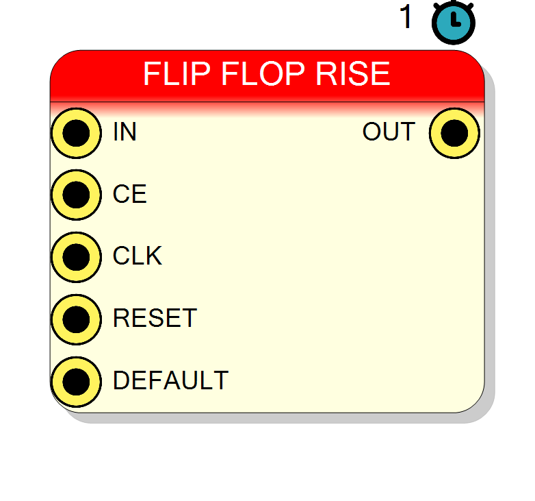
Introduction
This block implements a D-type flip-flop that captures data on rising clock edges. Unlike level-sensitive latches, flip-flops are edge-triggered, providing clean timing isolation between input and output.
The flip-flop operates as follows:
- On rising clock edge (↑) with CE = ‘1’: Output = Input
- Between clock edges: Output holds its value (input changes are ignored)
Key characteristics:
- Edge-triggered operation (samples only on rising edges)
- Clock enable for conditional updates
- Synchronous reset with configurable preset value
- Latency: 1 clock cycle
- Preferred over latches for synchronous digital design
Pin Description
Clock Enable input (active high).
- CE = ‘1’: Flip-flop samples IN on rising edges
- CE = ‘0’: Flip-flop holds current OUT value Default: ‘1’ if left unconnected.
Properties
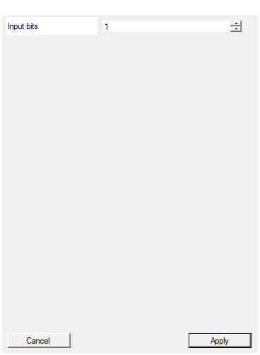
Set the number of bits of the input
Number of bits in the flip-flop (width of IN, DEFAULT, and OUT). Range: 1-2048 bits.Default: 1
Range: 1 – 2048
Functional description
A D flip-flop is an edge-triggered storage element that captures its input value only at clock edges. This component implements the following behavior:
Truth table
| CLK | CE | RESET | Behavior |
|---|---|---|---|
| X | X | 1 | OUT = PRESET (next ↑) |
| ↑ | 1 | 0 | OUT = IN |
| ↑ | 0 | 0 | OUT = OUT(previous) |
| ↓,— | X | 0 | OUT = OUT(previous) |
Edge-triggered sampling
The flip-flop samples its input only at the rising edge of the clock:
- Input is captured precisely at the clock transition
- Changes on IN between clock edges have no effect
- Provides timing isolation: input and output are separated by a register stage
Clock enable operation
The CE (Clock Enable) input allows conditional updates:
- CE = ‘1’: Flip-flop captures new data on rising edges
- CE = ‘0’: Flip-flop holds current value (input ignored)
This is useful for:
- Implementing enable signals in datapaths
- Creating gated registers
- Controlling when data should be updated
Reset and preset
The component supports synchronous reset:
- When RESET = ‘1’: Output is set to the PRESET value on the next rising clock edge
- PRESET input defines the reset state (can be any value, not just zero)
- Reset is synchronous: it requires a clock edge to take effect
Flip-flop vs Latch
Flip-flops (this component):
- Edge-triggered: sample only at clock transitions
- Provide clean timing isolation
- Standard for synchronous digital design
- No transparency issues
Latches:
- Level-sensitive: transparent when enabled
- Can propagate glitches
- Require careful timing analysis
- Used in specific applications only
Timing
| Property | Latency (clock cycles) |
|---|---|
| D Flip-Flop Rising | 1 |
The output updates exactly one clock cycle after the input is sampled.
Typical use cases
- Pipeline registers in datapath circuits
- State machines: storing current state
- Synchronous FIFOs: data storage elements
- Clock domain isolation: registering signals between clock domains
- Signal synchronization: two-stage synchronizers for async inputs
- Control registers: storing configuration values
- Data buffering: temporary storage in processing pipelines
Design best practices
- Setup and hold times: Ensure input data is stable around the clock edge
- Reset strategy: Use synchronous reset for better timing closure
- Clock enable: Prefer CE over clock gating for power management
- Fanout: Replicate heavily-loaded flip-flops to reduce fanout
- Initialization: Always provide a reset mechanism for predictable power-up state
Waveform example
Example with Input Size = 8 bits, showing edge-triggered operation:
Note:
- At time 1: OUT = A (sampled on rising edge, CE = 1)
- At time 2: OUT = A (held, CE = 0, B ignored)
- At time 3: OUT = C (sampled on rising edge, CE = 1)
- At time 5: OUT = D (sampled on rising edge, CE = 1)