
Gate and Delay (SW)
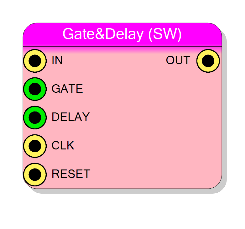
Programmable gate and delay block that delays an input pulse and stretches its width. The DELAY input controls output delay, while the GATE input controls output pulse width (both in clock cycles). Uses block RAM for efficient delay storage. Ideal for creating delayed, width-adjusted trigger signals.
Introduction
This block implements combined gate and delay functionality, delaying an input pulse by a programmable number of clock cycles and holding the output HIGH for a programmable gate width.
When IN goes HIGH:
- Output is delayed by DELAY clock cycles
- Output stays HIGH for GATE clock cycles
- Then returns LOW
Pin Description
Properties
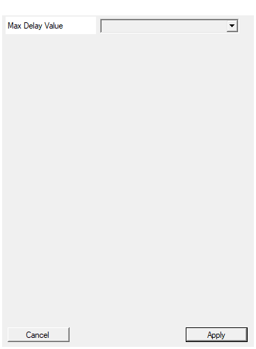
Set the amount of memory to reserve for this delay line
Maximum delay capacity. Allowed values: 64-65536. Reserves block RAM for delay line storage.Default: 1024
Options: 64 128 256 512 1024 2048 4096 8192 16384 32756 65536
Functional description
The component combines a programmable delay line with a pulse width controller. When a rising edge is detected on IN, the block:
- Delays the pulse by DELAY clock cycles
- Asserts OUT=1 for GATE clock cycles
- Returns OUT=0
Typical application
Converts narrow input pulses into wider, delayed output pulses for trigger logic.
Timing
Latency = DELAY + 1 cycles (inherent delay line latency). Output width = GATE cycles.
Typical use cases
- Trigger signal conditioning
- Pulse width adjustment for logic gates
- Delayed gate generation for coincidence windows