
RF NCO (programmable FTW)
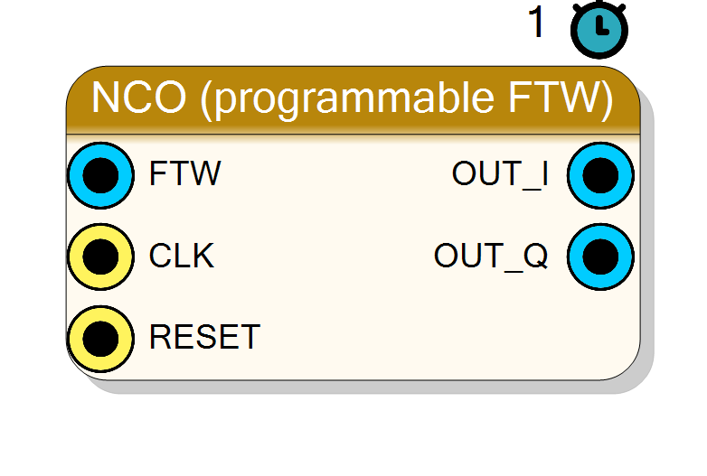
Numerically Controlled Oscillator with a run-time programmable frequency. Same core as Component_NCO but the FTW is exposed as a top-level input pin, so the fabric (or the SDK via a register bank) can retune the oscillator at any time.
Introduction
Identical to Component_NCO except that the Frequency Tuning Word is a top-level input pin instead of a synthesis-time constant. Wire it from a register slave in your design (SDK / register-file style) and you get a software-tunable LO.
FTW ─┐
│ ┌─────┐
├─►│ NCO ├── OUT_I / OUT_Q (complex tone)
CLK ─┘ └─────┘
Pin Description
f_norm = unsigned(FTW) / 2^AccSize.
Properties
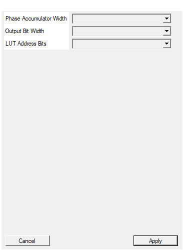
Bit width of the phase accumulator. Sets both the frequency resolution and the FTW bus width.
Bit width of the phase accumulator, which is also the width of theFTW bus. Default 32.
Default: 32
Options: 16 20 24 28 32 40 48
Bit width of each I / Q output sample (signed)
Bit width of each signed I / Q output sample. Range 8..24, default 16.Default: 16
Options: 8 9 10 11 12 13 14 15 16 17 18 19 20 21 22 23 24
log2 of the sin/cos LUT depth. Default 10 -> 1024 entries.
log2 of the sin/cos ROM depth. Default 10 (1024 entries).Default: 10
Options: 8 9 10 11 12
Usage
FTW bus
FTW is an unsigned AccSize-bit std_logic_vector. The relationship
between FTW and the emitted frequency is
f_norm = unsigned(FTW) / 2^AccSize (cycles / sample)
f = f_norm * Fs (Hz)
Interpretation is unsigned modulo 2^AccSize : setting FTW = 2^(AccSize-1)
gives exactly Fs/2 (Nyquist) — anything higher aliases back.
Inside the HLS core the FTW port is declared ap_stable, meaning:
- the accumulator samples it combinationally every clock,
- changes are visible on the output within one clock cycle,
- the value is not required to be stable across pipeline latency, so it can be updated at any time from the fabric.
Phase resolution and spurs
Same as Component_NCO : df/Fs = 1 / 2^AccSize, SFDR ~=
6 * LutAddrSize dB.
Firmware / driver helper
Converting a target frequency f (Hz) into an FTW word:
def freq_to_ftw(f_hz, fs_hz, acc_size):
return int(round((f_hz / fs_hz) * (1 << acc_size))) & ((1 << acc_size) - 1)
The Python testbench tb/nco/nco_tb.py uses exactly this formula.
Resources & Timing
-
Latency: 1 clock cycle
-
Throughput: 1 sample per clock (II=1)
Same footprint as Component_NCO : two ROMs + one adder. The FTW bus adds no logic beyond routing.