
RF Halfband Decimator (fixed)
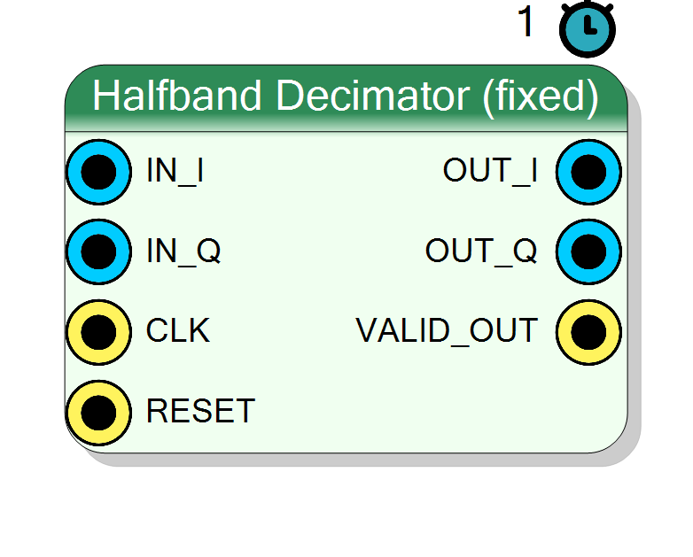
Complex I/Q halfband FIR filter that decimates by exactly 2 with coefficients computed by the plugin and baked into the netlist. The natural halfband cutoff sits at Fs/4, so it is the ideal anti-alias stage in front of a 2:1 rate reduction inside a multistage DDC.
Introduction
The Halfband Decimator (fixed) block filters a complex baseband stream (I and Q share the same real coefficients) and drops the sample rate by a factor of two. It is the workhorse rate-reduction stage of a multistage Digital Down-Converter (DDC).
A halfband FIR is a low-pass whose cutoff is placed exactly at Fs/4 (half of Nyquist). At that special frequency the impulse response has a remarkable property: every second coefficient is zero (except the single centre tap, which equals 0.5). The response is also symmetric. So roughly half of the multiplies are trivially zero and the rest come in symmetric pairs, which makes the halfband the cheapest possible FIR for a 2:1 decimation.
IN_I ─┐ fc = Fs/4 ┌── OUT_I (rate = IN rate / 2)
│ [ halfband ] │
IN_Q ─┘ h[even]=0 └── OUT_Q
└── VALID_OUT (1 every 2 in-clocks)
The coefficients are computed by the plugin at design time (windowed-sinc
at fc = 0.25*Fs, Hamming window, DC gain normalised to 1), quantised to
CoefSize signed bits and stored as a NumTaps * CoefSize bit constant
in the VHDL. They are not exposed to the fabric.
For a run-time programmable-coefficient version see
Component_HalfbandDecimatorProgrammable (halfband_decim_prog).
Pin Description
Properties
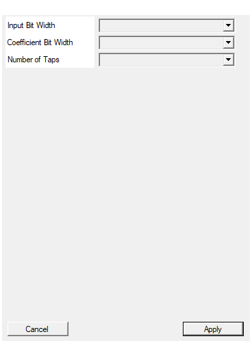
Bit width of each I/Q input sample (signed).
Bit width of each signed I / Q input sample. Range 4 to 32, default 16. Changing it triggers a redesign.Default: 16
Options: 4 5 6 7 8 9 10 11 12 13 14 15 16 17 18 19 20 21 22 23 24 25 26 27 28 29 30 31 32
Bit width of each coefficient (signed).
Bit width of each signed coefficient. Choices 10, 12, 14, 16, 18, 20, 24; default 16. A larger value lowers the stop-band error floor at the cost of DSP width.Default: 16
Options: 10 12 14 16 18 20 24
Number of taps. For a canonical halfband use lengths of the form 4k+3 (11, 15, 19, 23, 27, 31, …); the plugin will use whatever value you set as a plain FIR + downsample-by-2 anyway.
Number of filter taps (filter order =NumTaps - 1). Choices
7, 11, 15, 19, 23, 27, 31, 39, 47, 63; default 15. Use a
canonical halfband length of the form 4k+3 so the even taps fall
exactly on the sinc zeros. More taps sharpen the transition band at
the Fs/4 edge at the cost of DSPs and delay-line depth.
Default: 15
Options: 7 11 15 19 23 27 31 39 47 63
Usage
Why halfbands are the efficient DDC stages
A wideband receiver rarely decimates by a large factor in one FIR. Instead it cascades cheap 2:1 halfband stages (optionally after a CIC) because:
- The Fs/4 cutoff forces every other tap to zero -> ~half the DSP slices.
- Symmetry (
h[k] = h[N-1-k]) folds the remaining taps into pairs. - Each stage only has to reject the half of the band that will alias when the rate halves; successive stages then narrow the band progressively.
This block performs the decimation as a plain direct-form FIR evaluated every input clock, keeping the output only on every second input clock. Because the coefficients are compile-time constants, Vivado prunes the zero (and +/-1) taps automatically, so you get the halfband saving without any special hardware.
Mathematical model
For each channel c in {I, Q}, the filter computes at every input
sample n
acc_c[n] = sum_{k=0..NumTaps-1} h[k] * x_c[n-k]
and outputs y_c[m] = acc_c[2m] — i.e. it keeps one result out of two.
Coefficient generation (fixed variant)
h_ideal[n] = 2*fc * sinc(2*fc*(n - (N-1)/2)), fc = 0.25
w[n] = 0.54 - 0.46 * cos(2*pi*n / (N-1)) (Hamming)
h[n] = h_ideal[n] * w[n]
then normalised so sum h[n] = 1 (unity DC gain) and quantised to a
signed CoefSize-bit integer (scale 2^(CoefSize-1) - 1). Because
sinc(0.5*integer) = 0, the even-offset taps vanish automatically — you
do not have to hand them the zeros. For a canonical halfband use a tap
count of the form 4k+3 (11, 15, 19, 23, 27, 31, …).
Bit widths
Data is treated as signed two’s complement.
IN_I,IN_Q: signedInputSizebits.- internal product :
InputSize + CoefSizebits. OUT_I,OUT_Q: signedInputSize + CoefSize + 8bits.
The extra 8 accumulator bits (ACC_GROWTH = 8) absorb the tap sum without
overflow up to 256 taps. Truncate downstream if fewer bits are needed.
VALID_OUT / strobe behaviour
The core is pipelined at II=1 and is clocked at the input (fast)
rate — a new IN_I/IN_Q pair is accepted every clock. VALID_OUT is an
output strobe that is asserted on exactly every other clock to mark
the cycles on which OUT_I/OUT_Q carry a fresh, decimated sample; on the
intervening clocks the outputs hold their previous value and VALID_OUT
is low. After reset the internal keep flag starts true, so the first
post-reset output is a valid one. Downstream logic must gate on
VALID_OUT to run at the halved rate.
Latency and reset
#pragma HLS PIPELINE II=1: accepts one input pair per clock.- 1-clock reported latency (delay-line update + MAC tree + output reg).
- All data ports use the
ap_noneinterface (no ready/valid handshake); the coefficient bus usesap_stable. RESETis the HLS synchronous reset (ap_rst); it clears the delay lines and re-arms thekeepphase.
Typical applications
- Final / intermediate 2:1 stage of a multistage DDC, after the CIC and its compensation FIR.
- Anti-alias + rate halving anywhere a complex stream must be brought down by two before further processing.
- Cascade several instances back-to-back for /4, /8, /16 … decimation.
Resources & Timing
-
Latency: 1 clock cycle (reported)
-
Throughput: Accepts 1 input pair per clock (II=1); emits 1 valid output pair every 2 input clocks (output rate = input rate / 2).
Implemented with Vitis HLS. The delay lines and coefficient array are fully partitioned and the MACC loop is unrolled, so up to NumTaps DSP48 slices per channel are inferred. Because the coefficients are compile-time constants, Vivado optimises away the ~half of taps that are zero (and the +/-1 taps), realising the classic halfband DSP saving with no special structure. Fixed 2:1 rate change is built into the block.