
Scaler (Even Division)
Programmable frequency divider (scaler) that divides input clock frequency by even integer divisors only (2, 4, 6, 8, …). The SCALE input is an index where division factor = SCALE × 2. Generates output with 50% duty cycle. Supports bypass mode (SCALE=0). Operates up to 400 MHz.
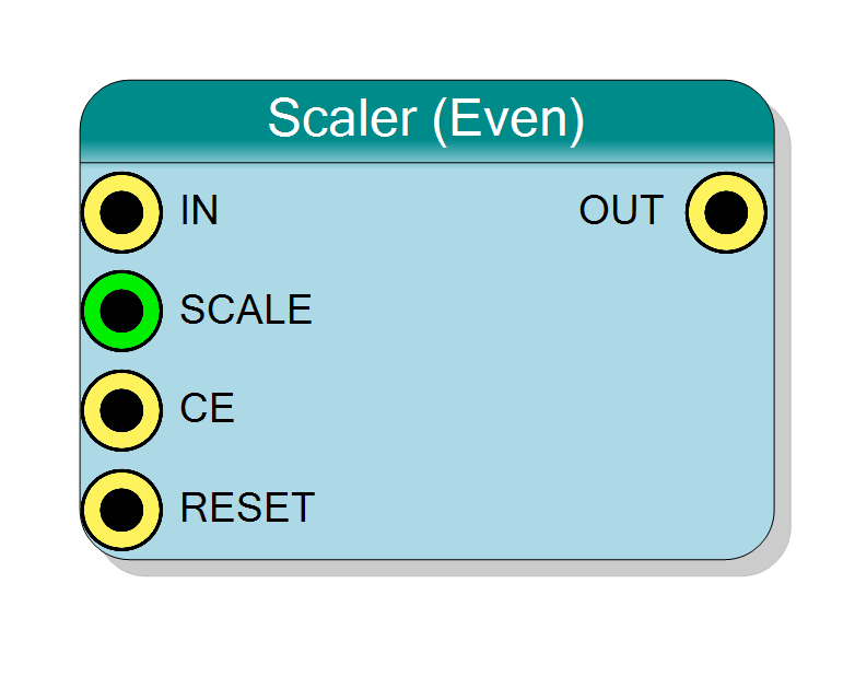
Introduction
This block implements a programmable frequency divider that generates an output clock at a divided frequency with guaranteed 50% duty cycle.
Key features:
- Divides input frequency by even integers only (2, 4, 6, 8, 10, …)
- 50% duty cycle output
- Runtime-programmable via SCALE index input
- Clean, glitch-free output transitions
- Bypass mode when SCALE=0
Operation:
$$ f_{\text{OUT}} = \frac{f_{\text{IN}}}{\text{SCALE} \times 2} $$
Where SCALE is an integer index (0, 1, 2, 3, …) that determines the division factor.
Division factor = SCALE × 2 (always even)
Output toggles every SCALE input cycles, producing 50% duty cycle.
Special case: SCALE=0 bypasses the divider (OUT follows IN directly).
Pin Description
Input clock to be divided.
Typically connected to system clock or another clock source.
Frequency range: Limited only by FPGA capabilities (typically DC to several hundred MHz).
Requirements:
- Clean clock signal
- Stable frequency for predictable output
This signal clocks the internal divider logic.
Default: Connects to global clock if left unconnected.
Scale index (determines division factor).
Type: INTEGER (VHDL signed 32-bit integer)
Formula: Division factor = SCALE × 2
Valid values:
- SCALE=0: Bypass mode (no division, OUT follows IN)
- SCALE=1: Divide by 2 (f_OUT = f_IN / 2)
- SCALE=2: Divide by 4 (f_OUT = f_IN / 4)
- SCALE=3: Divide by 6 (f_OUT = f_IN / 6)
- SCALE=N: Divide by N×2 (f_OUT = f_IN / (N×2))
Range: 0 to 2^31 - 1 (INTEGER type range)
Examples @ 100 MHz input:
- SCALE=0 → 100 MHz (bypass)
- SCALE=1 → 50 MHz (÷2)
- SCALE=5 → 10 MHz (÷10)
- SCALE=50 → 1 MHz (÷100)
Dynamic change: Can be changed at runtime. New value takes effect at next counter rollover. For glitch-free change, assert RESET after changing SCALE.
Constant value: Can connect to constant if fixed division needed.
Width: 32 bits (INTEGER)
Clock enable (active high).
- ‘1’ = Scaler enabled, output toggles normally
- ‘0’ = Scaler frozen, output holds current state
When CE=‘0’:
- Internal counter stops
- Output holds last value
- Resumes counting when CE=‘1’ again
Useful for:
- Gating output clock
- Power saving
- Synchronizing multiple scalers
Default: Connects to ‘1’ if left unconnected (always enabled).
Synchronous reset (active high).
- ‘1’ = Reset scaler: counter to 0, output to ‘0’
- ‘0’ = Normal operation
Use cases:
- Initialize output to known state
- Synchronize output phase with system
- Glitch-free SCALE value change (reset before changing)
- Align multiple scalers
Synchronous to IN clock.
Default: Connects to global reset if left unconnected.
Divided clock output.
Frequency: f_OUT = f_IN / (SCALE × 2)
Duty cycle: 50% (guaranteed when SCALE > 0)
- High time = SCALE × T_IN
- Low time = SCALE × T_IN
- Period = (SCALE × 2) × T_IN
- Division factor = SCALE × 2 (always even)
Bypass mode (SCALE=0): OUT follows IN directly
Phase: Output transitions aligned to IN rising edges
Initial state: ‘0’ after reset
Properties:
- Registered output (glitch-free)
- Suitable for use as clock signal
- Can drive clock networks
- Edges synchronous to IN
Example (SCALE=2, f_IN=100MHz):
- Division factor = 2 × 2 = 4
- f_OUT = 100 MHz / 4 = 25 MHz
- High for 2 IN cycles (20 ns)
- Low for 2 IN cycles (20 ns)
- Period = 4 IN cycles (40 ns)
Properties
This component has no configurable properties.
Division factor is set at runtime via the SCALE input port.
SCALE can be connected to:
- Constant value for fixed division
- Register/signal for runtime-programmable division
- Control logic for dynamic frequency selection
Functional description
The scaler implements a modulo-SCALE counter that toggles output every SCALE cycles:
Operation principle
- Internal counter counts 0 to (SCALE - 1)
- When counter reaches (SCALE - 1):
- Toggle output
- Reset counter to 0
- Output transitions occur every SCALE input cycles
- Complete output period = SCALE × 2 input cycles
- Division factor = SCALE × 2
Mathematical model
$$ \text{OUT}(n) = \begin{cases} \overline{\text{OUT}(n-1)} & \text{if } \text{counter} = \text{SCALE} - 1 \ \text{OUT}(n-1) & \text{otherwise} \end{cases} $$
Bypass mode (SCALE=0)
When SCALE=0, the scaler is bypassed and OUT follows IN directly (no division).
Even division only
Why only even divisors?
- Output toggles every SCALE cycles
- Complete period = SCALE × 2 cycles (always even)
- 50% duty cycle: High time = SCALE cycles, Low time = SCALE cycles
- Division factor = SCALE × 2 (always even)
For odd divisors or arbitrary division factors, use Fractional Scaler component instead.
Frequency division examples
| SCALE | Division Factor | Input Freq | Output Freq | High Time | Low Time |
|---|---|---|---|---|---|
| 0 | 1 (bypass) | 100 MHz | 100 MHz | follows IN | follows IN |
| 1 | 2 | 100 MHz | 50 MHz | 1 cycle | 1 cycle |
| 2 | 4 | 100 MHz | 25 MHz | 2 cycles | 2 cycles |
| 3 | 6 | 100 MHz | 16.67 MHz | 3 cycles | 3 cycles |
| 4 | 8 | 100 MHz | 12.5 MHz | 4 cycles | 4 cycles |
| 5 | 10 | 100 MHz | 10 MHz | 5 cycles | 5 cycles |
| 50 | 100 | 100 MHz | 1 MHz | 50 cycles | 50 cycles |
| 500 | 1000 | 100 MHz | 100 kHz | 500 cycles | 500 cycles |
Timing diagram
For SCALE=2 (divide-by-4):
- Counter: 0, 1, 0, 1, … (counts 0 to SCALE-1 = 1)
- OUT toggles every 2 cycles (when counter reaches SCALE-1)
- Output period = 4 input cycles (SCALE × 2)
- Division factor = 4
Typical use cases
- Clock generation: Generate slower clocks from system clock
- Sampling clock: Create ADC/DAC sampling clocks
- Baud rate generation: Generate UART baud clocks
- Timing reference: Create timing bases for slower logic
- Frequency synthesis: Part of frequency synthesis chains
- Test clock generation: Generate test clocks at various frequencies
Design considerations
Scale factor selection
Minimum SCALE: 0 (bypass, no division) Typical range: 1 to 2^31 - 1 (INTEGER type)
Common values:
- SCALE=0: Bypass (division factor = 1)
- SCALE=1: Division by 2 (50 MHz from 100 MHz)
- SCALE=5: Division by 10 (10 MHz from 100 MHz)
- SCALE=50: Division by 100 (1 MHz from 100 MHz)
- SCALE=500: Division by 1000 (100 kHz from 100 MHz)
Output frequency calculation
$$ f_{\text{OUT}} = \frac{f_{\text{IN}}}{\text{SCALE} \times 2} $$
$$ T_{\text{OUT}} = \text{SCALE} \times 2 \times T_{\text{IN}} $$
Examples @ 100 MHz input:
- SCALE=0: 100 MHz output (bypass)
- SCALE=1: 50 MHz output (÷2)
- SCALE=5: 10 MHz output (÷10)
- SCALE=50: 1 MHz output (÷100)
- SCALE=500: 100 kHz output (÷1000)
Changing SCALE dynamically
SCALE can be changed at runtime:
- New value takes effect on next counter rollover
- May cause one irregular output period during transition
- For glitch-free changes, assert RESET before changing SCALE
Duty cycle accuracy
Output duty cycle = 50% ± clock jitter (when SCALE > 0)
- High time exactly = Low time = SCALE input periods
- No cumulative error
- Output edges aligned to input clock
- Bypass mode (SCALE=0): Output follows input directly
Resource usage
- One counter: ceil(log2(SCALE_max)) bits wide
- One flip-flop for output
- One comparator
- Minimal FPGA resources
For SCALE input up to 1000:
- Counter: 10 bits (log2(1000) ≈ 10)
- Total: ~11 flip-flops + comparator
Output as clock
Output can drive clock networks:
- Clean transitions (registered)
- 50% duty cycle suitable for clocking
- Use dedicated clock routing resources
- Consider clock skew/jitter in timing analysis
Comparison with Fractional Scaler
| Feature | Scaler (Even) | Fractional Scaler |
|---|---|---|
| Division factor | Even only (2,4,6…) | Any integer |
| Control input | Index (SCALE) | Direct divisor |
| Formula | Div = SCALE × 2 | Div = VALUE |
| Duty cycle | Always 50% | Approximate 50% |
| Complexity | Very simple | More complex |
| Max frequency | Up to 400 MHz | Lower |
| Best for | Even division | Odd division |