
Programmable Left Shift [TM]
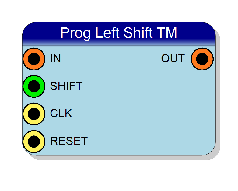
Time-multiplexed programmable bitwise left shift operation. Shifts all bits of the input binary number to the left by a dynamically programmable amount via the SHIFT input port. Fills vacant rightmost positions with zeros. Supports configurable maximum shift and TM factors from 2 to 32. Optionally latched output (configurable latency: 0 or 1 clock cycle).
Introduction
This block performs a programmable left shift operation on time-multiplexed (TM) data streams. Unlike fixed shift operations, the shift amount is dynamically controlled via the integer SHIFT input port, allowing runtime flexibility.
Each bit of the input is shifted left by the amount specified on the SHIFT port (0 to Max Shift), and zeros are inserted in the vacant rightmost positions.
The shift operation can be:
- Combinational (zero latency, Latch Output = false)
- Registered (1 clock cycle latency, Latch Output = true)
$$ \mathrm{OUT}(n) = \mathrm{IN}(n) \ll \mathrm{SHIFT}(n), $$
where SHIFT is the runtime-configurable shift amount. The TM Factor property determines how many parallel samples are processed per clock cycle.
Pin Description
Input Width × TM Factor
Each TM phase receives its corresponding slice of the input bus.
Shift amount control (integer input). Specifies how many bit positions to shift left. Range: 0 to Max Shift (configurable property) Type: Integer (non-TM, applies to all TM phases)
Values outside [0, Max Shift] may produce undefined results.
Clock input for registered output mode. Only used when Latch Output = true. Defaults to acquisition clock (CLK_ACQ).
On rising edge, the shifted result is latched to OUT.
Reset input for registered output mode. Only used when Latch Output = true. Defaults to global reset.
When asserted, clears the output register to zero.
Left-shifted output, always TM (same factor as IN).
Width: Input Width × TM Factor (same as IN)
Latency:
- 0 cycles if Latch Output = false (combinational)
- 1 cycle if Latch Output = true (registered)
Properties
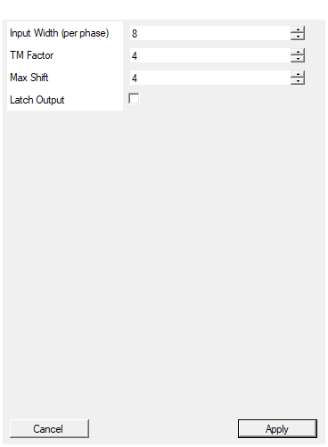
Set the input word size in bits per phase
Number of bits per input sample ($N_\text{in}$). Range: 1 – 128. Each TM phase processes samples of this width. Output width is always equal to input width.Default: 8
Range: 1 – 128
Set the time multiplexing factor (number of phases)
Time-multiplexing factor (number of parallel phases). Allowed values: 2, 4, 8, 16, 32 (up to 32). Higher values increase throughput proportionally but consume more FPGA resources (one barrel shifter instance per TM phase).Default: 4
Range: 2 – 32
Maximum shift value
Maximum allowed shift amount ($S_\text{max}$). Range: 1 – 16. The SHIFT input must be in the range [0, Max Shift].
Larger Max Shift values require more FPGA resources (wider barrel shifter). Choose the smallest value that meets your application needs.
Default: 4
Range: 1 – 16
If true, output is registered (latched)
Output register control (boolean).
- false (default): Combinational output, zero latency
- true: Registered output, 1 clock cycle latency
Enable latching when:
- Timing closure is difficult
- Pipelining is needed for high-speed operation
- Synchronous output alignment is required
Default: False
Functional description
The component implements a programmable barrel shifter (left shift) in VHDL, replicated N times (where N = TM Factor) to support time-multiplexed data streams.
For each TM phase, the operation is:
$$ y[i] = x[i] \ll s, $$
where:
- $x[i]$ → input sample at phase $i$
- $y[i]$ → output sample at phase $i$
- $s$ → shift amount from SHIFT input (0 to Max Shift)
The programmable left shift appends $s$ zero bits to the right:
$$ y = x \times 2^s \mod 2^{W} $$
where $W$ is the word width (output is same width as input, MSBs discarded if overflow).
Dynamic shift control
- SHIFT port: Integer input specifying the shift amount (range: 0 to Max Shift)
- Barrel shifter: Efficiently implements any shift from 0 to Max Shift
- Same width: Output width always equals input width (overflow bits discarded)
Latency modes
The block offers two latency configurations via the Latch Output property:
-
Latch Output = false (default):
- Purely combinational logic
- Latency = 0 clock cycles
- Output changes immediately with inputs
-
Latch Output = true:
- Output is registered (latched) on CLK rising edge
- Latency = 1 clock cycle
- Provides timing closure for high-speed designs
- RESET clears the output register
Example
Given an 8-bit input and Max Shift = 4:
- Input =
10110011, SHIFT = 0 → Output =10110011(no shift) - Input =
10110011, SHIFT = 2 → Output =11001100(shift left 2) - Input =
10110011, SHIFT = 4 → Output =00110000(shift left 4, MSBs discarded)
Mathematical background
Programmable left shift by $s$ positions is equivalent to multiplication by $2^s$ modulo word width:
$$ x \ll s = (x \times 2^s) \mod 2^W $$
This is commonly used for:
- Dynamic scaling in fixed-point arithmetic
- Runtime-configurable multiplication by powers of 2
- Bit alignment operations with variable offset
- Building adaptive signal processing algorithms
Timing
The component latency depends on the Latch Output property:
| Property | Latch Output = false | Latch Output = true |
|---|---|---|
| Programmable Left Shift TM | 0 | 1 |
All TM phases are processed in parallel within the same clock cycle.
Typical use cases
- Variable-gain amplification (multiply by 2^N)
- Adaptive fixed-point rescaling
- Dynamic bit field packing with configurable offsets
- Building configurable DSP pipelines
- Barrel shifter components in ALUs
Waveform example
Example with TM Factor = 4, Max Shift = 4, Input = 4-bit values, SHIFT = 2, Latch Output = false.
Note: With Latch Output = false, output is immediate (combinational). Values in hex: 0x5 « 2 = 0x14 → 0x4 (4-bit truncated), 0x7 « 2 = 0x1C → 0xC, etc.