Getting Started with DT5550
Comprehensive step-by-step tutorial for creating a DT5550 firmware project. Learn to build a complete signal processing system with signal generation, trigger discrimination, time-over-threshold measurement, and oscilloscope readout using SCI-Compiler’s graphical programming environment.
Introduction
This tutorial demonstrates how to design firmware for the DT5550 board that implements a complete signal processing and measurement system. You’ll create a project that generates test signals, discriminates pulses with a trigger, measures time-over-threshold, and visualizes results with an oscilloscope.
What You’ll Build
The firmware you create will include:
- Signal Generator – Produces shaped exponential test signals
- Leading Edge Trigger – Discriminates signals above a threshold
- Time-over-Threshold (ToT) Measurement – Measures pulse width
- Event Counter – Counts total number of triggers
- Oscilloscope – Real-time waveform visualization
- Registers – Runtime parameter control via Resource Explorer
Learning Objectives
By completing this tutorial, you will learn:
- Creating projects for DT5550 hardware
- Using logic blocks (counters, edge detectors, chronometers)
- Implementing signal processing chains
- Creating and using registers for control and readout
- Testing firmware with Resource Explorer
- Measuring timing characteristics
Prerequisites
Before starting, ensure you have:
- ✓ SCI-Compiler installed and licensed for DT5550
- ✓ DT5550 hardware available
- ✓ Xilinx Vivado installed (for local compilation)
- ✓ Basic familiarity with SCI-Compiler interface
Step 1: Create the Project
Launch SCI-Compiler and create a new project for the DT5550 board.
Create New Project
- Run SCI-Compiler
- In the starting window, click the DT5550 button
- Enter a project name (e.g.,
DT5550_ToT_Tutorial) - Specify or browse to a project folder destination
- Click Create
A blank diagram workspace will open for your design.
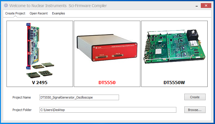
Figure 1: Creating a new DT5550 project
Step 2: Create the Registers
Define three registers to control the trigger threshold and read measurement results.
Add Registers via Memory Mapping
- Click the Memory Mapping tab at the bottom of the window
- For each register:
- Enter the register name in the text field
- Click Add
Create these three registers:
- Threshold – Controls trigger discrimination level
- TriggerCounts – Reads total number of triggers
- TimeOverThreshold – Reads ToT measurement (in clock cycles)
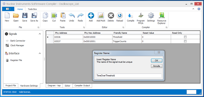
Figure 2: Creating registers in Memory Mapping tab
These registers will be automatically assigned memory addresses and accessible from Resource Explorer.
Step 3: Add the Signal Generator
Add a block to generate test signals for the demonstration.
Insert Signal Generator Block
- Select the Tools Box toolbar
- In the Logic group, click Delay Memory
- From the submenu, select Signal Generator
Configure Signal Generator
A configuration window will appear. Set parameters as follows:
- Shape: Shaped exponential
- Samples: 4096
- Rise Time: 100
- Decay Time: 1000
- Amplitude: 32767
- OFFSET (Sample): 800
- Name: SigGen or similar
Click Apply to add the block to the diagram.
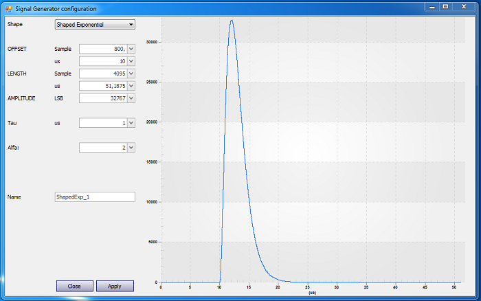
Figure 3: Configuring the Signal Generator block
What this does:
- Generates a repeating exponential decay pulse
- Offset of 800 samples provides pretrigger region
- Output is a 16-bit signed signal
Step 4: Add the Leading Edge Trigger
Add a trigger to discriminate signals above a threshold.
Insert Trigger Block
- In the Tools Box toolbar, go to Signal Processing group
- Click DAQ
- Select Trigger (Leading Edge)
Configure the Trigger
Set the following parameters:
- Input Width: 16 bits (match signal generator)
- Threshold Width: 16 bits
- Polarity: Positive
- Name: Trigger_LE or similar
Click OK to create the block.
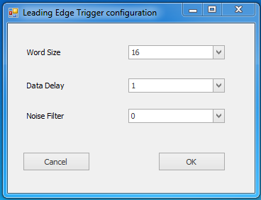
Figure 4: Configuring Leading Edge Trigger
Connect Signal to Trigger
Connect the OUT pin of the Signal Generator to the In pin of the Trigger block.
Add Threshold Register
The trigger needs a threshold value from a register:
- Click Register menu in the Communication group
- Select Register (Read)
- In the configuration window:
- Select the Threshold register
- Set Mode: Bit Vector
- Set Size: 16
- Click OK
Connect the Threshold output of the register block to the Threshold input of the Trigger.
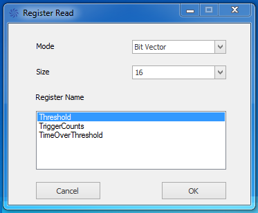
Figure 5: Adding and configuring Threshold register
Step 5: Add the Oscilloscope
Add an oscilloscope endpoint to visualize the signals.
Insert Oscilloscope Block
- In the DAQ submenu, click Oscilloscope
- Configure parameters:
- Number of Channels: 1
- Buffer Size: 4096 (match signal generator samples)
- Data Width: 16
- Analog Inputs: 1
- Digital Inputs: 1 (for ToT signal)
Click OK to add the block.
Make Connections
Connect the following signals:
- Signal Generator OUT → Oscilloscope A1 (analog input)
- Trigger TOT → Oscilloscope D0 1 (digital input)
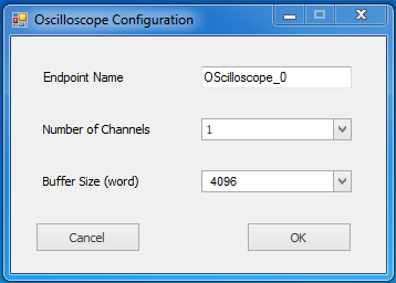
Figure 6: Oscilloscope configuration and connections
What you’ll see:
- Analog trace shows the exponential signal
- Digital trace shows when signal is above threshold (ToT)
Step 6: Add the Counter
Count the total number of trigger events using a counter block.
Insert Counter Block
- In the Logic group, click Timer Counters
- Select Counter (Rising Edge)
- Add the block to the diagram
Connect Trigger to Counter
Connect the Trigger output pin of the Trigger block to the In input pin of the Counter.
Add Constant TRUE Block
The counter needs an always-high enable signal:
- Click Misc button
- Select True
- A constant TRUE block appears
Connect the TRUE block output to the GATE input of the Counter (enables counting).
Add TriggerCounts Register (Write)
Create a register to read the count value:
- Click Register menu
- Select Register (Write)
- Configure:
- Select TriggerCounts register
- Mode: Bit Vector
- Size: 32
- Click OK
Make Final Counter Connections
- Counter Counts → TriggerCounts register input
- TRUE block → TriggerCounts register WR pin (write enable)
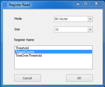
Figure 7: Counter block with TriggerCounts register
Function:
- Counts every trigger event
- Value continuously written to register
- Readable via Resource Explorer
Step 7: Add the Chronometer (Time-over-Threshold Measurement)
Measure the duration that the signal exceeds the threshold using a chronometer.
Understanding ToT Measurement
The Trigger block’s TOT output is high when the input signal exceeds the threshold. We’ll measure this pulse width in clock cycles using a Start/Stop Chronometer.
Insert Chronometer Block
- In Logic group, click Timer Counters
- Select Chronometer (Start/Stop)
- Add to diagram
Insert Edge Detector Blocks
We need to detect the rising and falling edges of the ToT signal:
- In Sequential Logic menu, add Edge Detector (Rising Edge)
- Add Edge Detector (Falling Edge)
Connect Edge Detectors
- Trigger TOT → Rising Edge Detector In
- Trigger TOT → Falling Edge Detector In
Add Pulse Width Constant
Edge detectors need a pulse width specification:
- Click Misc → Constant (int)
- Enter value: 1 (single clock cycle)
- Click OK
Connect the constant output to Pulse Width inputs of both edge detectors.
Connect Chronometer
- Rising Edge Detector OUT → Chronometer Start
- Falling Edge Detector OUT → Chronometer Stop
- Trigger Trigger → Chronometer Reset (reset after each event)
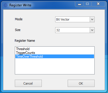
Figure 8: Chronometer and edge detector configuration
Add TimeOverThreshold Register
- Add a Register (Write) block
- Select TimeOverThreshold register
- Set Mode: Bit Vector, Size: 32
- Connect:
- Chronometer Time → TimeOverThreshold register input
- TRUE block → TimeOverThreshold WR pin
Function:
- Chronometer counts clock cycles between Start and Stop
- Result is the ToT duration in clock cycles
- Value continuously written to register
Step 8: Complete the Design
Your firmware design is now complete. The diagram should look like this:
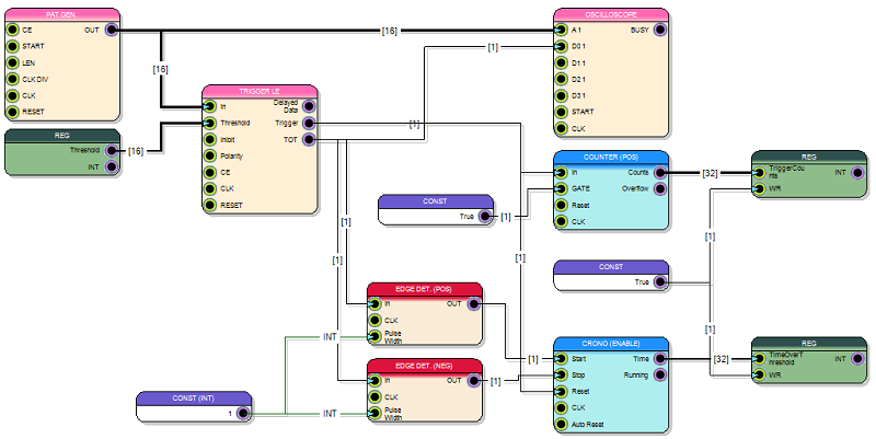
Figure 9: Complete firmware block diagram
Design Summary
| Block | Function |
|---|---|
| Signal Generator | Generates exponential test pulses |
| Leading Edge Trigger | Discriminates signals above threshold |
| Oscilloscope | Visualizes analog signal and ToT digital signal |
| Counter | Counts total triggers |
| Chronometer | Measures ToT duration in clock cycles |
| Registers | Threshold control, TriggerCounts readout, ToT readout |
Step 9: Compile the Firmware
Generate the FPGA bitstream from your block diagram.
Start Compilation
- Select the Home toolbar
- Press the Compile button
- SCI-Compiler executes Vivado in the background
- Monitor progress in the Compiler Output tab
Compilation time: Typically 30-60 minutes for DT5550 (Kintex-7 FPGA)
Check for Success
When complete, the Compiler Output will show:
Successful Compilation!
The .bit file is created in your project folder.
Troubleshooting:
- If errors occur, check all connections are complete
- Verify all input pins are connected
- Review error messages for specific issues
Step 10: Program the FPGA
Download the firmware to the DT5550 hardware.
Prepare Hardware
- Power on the DT5550
- Connect to your computer via:
- USB 3.0 (recommended), or
- Ethernet (if configured)
Program the Device
- Press the Program FPGA button in SCI-Compiler
- The tool automatically:
- Detects the programming cable
- Connects to the FPGA
- Downloads the bitstream
Verify Success
The Compiler Output will display:
Target device programmed successfully
The DT5550 is now running your custom firmware.
Step 11: Test with Resource Explorer
Use Resource Explorer to interact with the running firmware.
Launch Resource Explorer
Click the Resource Explorer button in the toolbar.
Connect to DT5550
In the Connection window:
- Select DT5550 board model
- Choose Connection Type (USB or Ethernet)
- Select correct Serial Number or IP address
- The Select Json File field auto-fills with the project’s JSON descriptor
- Click Connect
Resource Explorer will enumerate available resources:
- Registers (Threshold, TriggerCounts, TimeOverThreshold)
- Oscilloscopes (Oscilloscope_0)
- Other endpoints as defined
Step 12: Create a Register Table
Set up a table to view and control registers.
Create New Table
- Click View menu in Resource Explorer
- Select New Table
- Table 0 is created and displayed
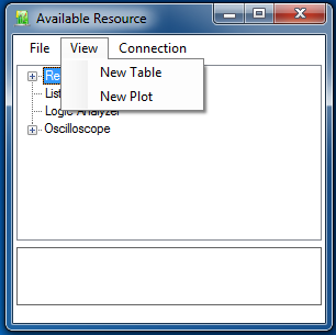
Figure 10: Creating a register table
Add Registers to Table
- Right-click on Registers in the tree
- Select Add All to Table
- In the “Choose Table” dialog, select Table 0
- Click Add to Table
All three registers appear in the table with their names and addresses.
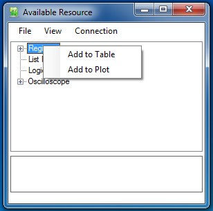
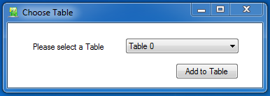
Figure 11: Adding registers to the table
Step 13: Control Threshold and Read Results
Interact with the firmware by setting the threshold and reading measurements.
Set Threshold to 1000
- In the Threshold row, locate the Value Write cell
- Ensure Format is set to Decimal
- Enter 1000
- Click the Set button
The threshold register is now set to 1000.
Read Measurements
Click the Get buttons for:
- TriggerCounts – Shows total number of triggers detected
- TimeOverThreshold – Shows ToT duration in clock cycles
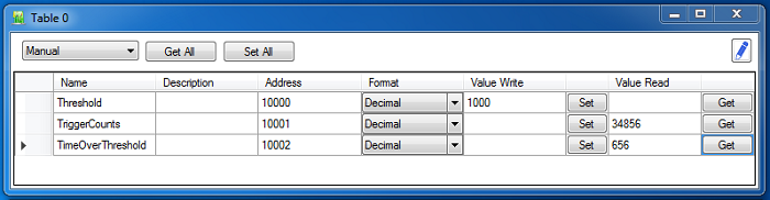
Figure 12: Register table with threshold = 1000
Calculate ToT in Nanoseconds
The DT5550 uses an 80 MHz clock:
- 1 clock cycle = 1 / 80 MHz = 12.5 ns
If TimeOverThreshold reads 656 cycles:
- ToT = 656 × 12.5 ns = 8200 ns = 8.2 µs
Step 14: View Waveforms in Oscilloscope
Visualize the signal and ToT in real-time.
Open Oscilloscope Viewer
- Right-click on Oscilloscope_0 in the Resource Explorer tree
- Select View
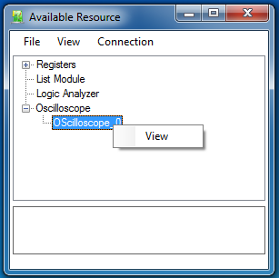
Figure 13: Opening Oscilloscope viewer
Configure Oscilloscope
Set the following parameters:
- Trigger Mode: Single (capture one waveform)
- Trigger Source: Channel 0 (analog input)
- Trigger Edge: Rising
- Trigger Level: 1000 (match threshold register)
Enable Channel 0 checkbox to display the signal.
Start Acquisition
Click the green arrow (▶) to start waveform capture.
View Results
The oscilloscope displays:
- Analog signal (exponential pulse)
- Digital signal (ToT indicator, scaled to analog maximum)
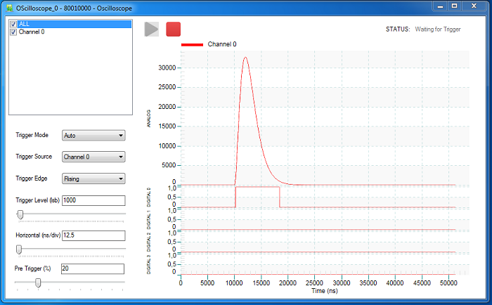
Figure 14: Oscilloscope showing signal and ToT with threshold = 1000
Observations:
- The ToT digital signal is high when analog exceeds 1000
- The ToT duration matches the TimeOverThreshold register value (~8200 ns)
Step 15: Experiment with Different Thresholds
Change the threshold to see how ToT duration varies.
Test Threshold = 10000
- In the register table, set Threshold to 10000
- Click Set
- Click Get on TimeOverThreshold
Result: 360 clock cycles = 4500 ns
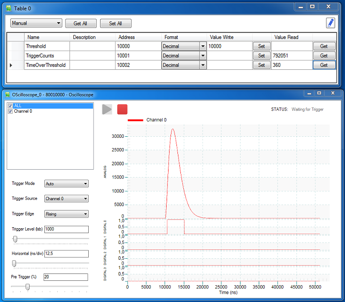
Figure 15: Results with threshold = 10000
Observation: Higher threshold = shorter ToT duration.
Test Threshold = 20000
- Set Threshold to 20000
- Read TimeOverThreshold: 228 cycles = 2850 ns
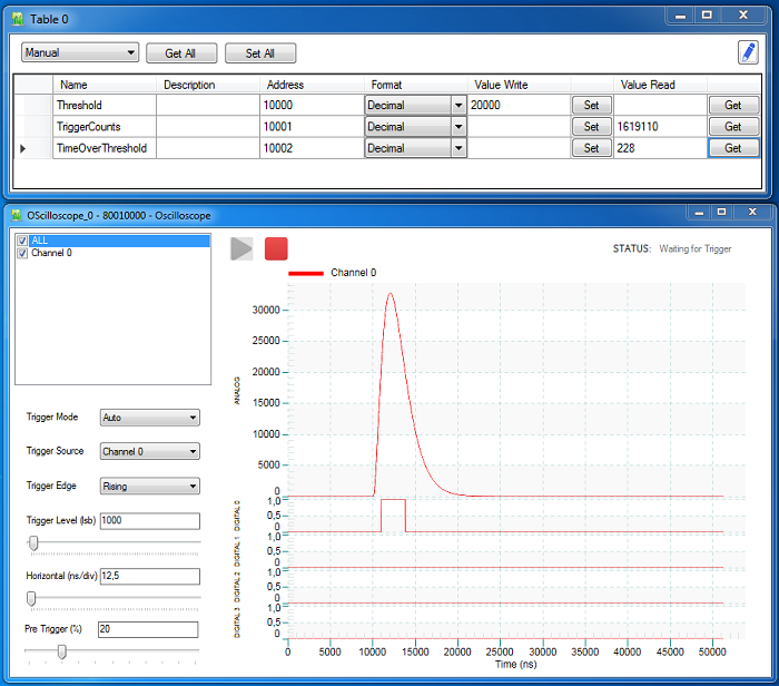
Figure 16: Results with threshold = 20000
Summary of Results
| Threshold | ToT (cycles) | ToT (ns) | ToT (µs) |
|---|---|---|---|
| 1000 | 656 | 8200 | 8.2 |
| 10000 | 360 | 4500 | 4.5 |
| 20000 | 228 | 2850 | 2.85 |
Conclusion: As expected, higher discrimination thresholds result in shorter time-over-threshold.
Understanding the Design
Signal Flow
Signal Generator
↓
[Exponential Pulse]
↓
Leading Edge Trigger ←── Threshold Register
↓
┌─────┴─────┐
↓ ↓
Trigger ToT Signal
↓ ↓
Counter Chronometer
↓ ↓
TriggerCounts TimeOverThreshold
Register Register
Trigger Output Signals
The Leading Edge Trigger provides two outputs:
- Trigger: Single-cycle pulse when signal crosses threshold (rising edge)
- TOT: High while signal exceeds threshold
Chronometer Operation
The Start/Stop Chronometer:
- Starts counting on rising edge of ToT (signal crosses threshold up)
- Stops counting on falling edge of ToT (signal crosses threshold down)
- Resets on each Trigger pulse (ready for next event)
- Outputs the Time (count) to the TimeOverThreshold register
Clock Frequency
DT5550 uses 80 MHz processing clock:
- Period = 12.5 ns
- All timing measurements are in multiples of 12.5 ns
Next Steps
Congratulations! You’ve built a complete signal processing system. Now explore further:
Add More Processing
-
Add a Baseline Restorer:
- Remove DC offset from signals
- Improves trigger stability
-
Add a Digital Shaper:
- Apply CR-RC or CR-RC² shaping
- Optimize signal-to-noise ratio
-
Add a Spectrum (MCA):
- Accumulate energy histogram
- Analyze pulse height distribution
-
Add a List Endpoint:
- Record event-by-event data
- Store ToT, timestamp, energy per event
Connect Real Hardware
-
Connect a detector to DT5550 inputs:
- Use the differential analog inputs
- Adjust input gain and offset
-
Replace Signal Generator with real ADC input:
- Remove Signal Generator block
- Use Board Pin → Analog In block
- Connect detector output
Advanced Topics
- Pile-up rejection: Detect overlapping pulses
- CFD trigger: Constant Fraction Discriminator for better timing
- Energy measurement: Trapezoidal filter, charge integration
- Coincidence logic: Multi-channel trigger correlation
Troubleshooting
Compilation Issues
Problem: Vivado reports errors
Solutions:
- Check all block inputs are connected
- Verify bit widths match (especially signals and registers)
- Review Compiler Output for specific error messages
- Ensure Memory Mapping was completed before compilation
Cannot Connect to DT5550
Problem: Resource Explorer fails to connect
Solutions:
- Verify DT5550 is powered on
- Check USB/Ethernet cable connection
- Ensure firmware was successfully programmed
- Try different USB port or cable
- Check firewall settings (for Ethernet connection)
Register Reads Show Zero
Problem: TriggerCounts or TimeOverThreshold always read 0
Solutions:
- Verify signal generator is running (check oscilloscope)
- Check threshold is lower than signal amplitude
- Ensure all connections to register blocks are correct
- Verify WR (write enable) pins are connected to TRUE block
Oscilloscope Shows No Trigger
Problem: Waveform won’t trigger
Solutions:
- Set Trigger Mode to “Free Running” to see if signal exists
- Check Trigger Level matches or is lower than signal amplitude
- Verify Trigger Edge is set correctly (Rising for positive pulses)
- Ensure Channel 0 is enabled/selected
Summary
This tutorial covered a complete DT5550 firmware development workflow:
| Phase | Tasks |
|---|---|
| Design | Created signal generator, trigger, counters, chronometer, oscilloscope |
| Register Control | Implemented threshold control and readout registers |
| Compilation | Generated FPGA bitstream using Vivado |
| Programming | Downloaded firmware to DT5550 |
| Testing | Used Resource Explorer to control and monitor firmware |
| Validation | Verified ToT measurements at multiple thresholds |
You now understand:
- ✓ DT5550 firmware development process
- ✓ Creating complex signal processing chains
- ✓ Using logic blocks (counters, edge detectors, chronometers)
- ✓ Implementing registers for control and readout
- ✓ Testing firmware with Resource Explorer
- ✓ Interpreting timing measurements
Continue exploring SCI-Compiler’s extensive block library to build custom FPGA firmware for your specific signal processing applications!