
Fixed Delay [TM]
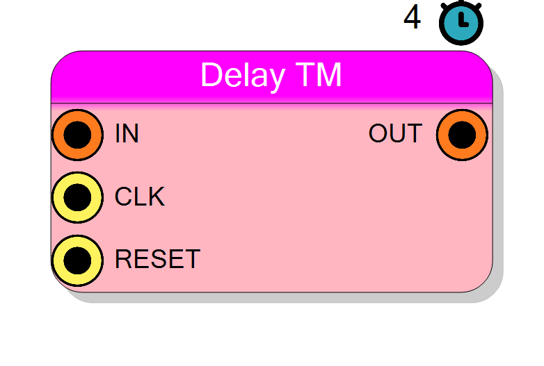
Time-multiplexed fixed delay line that delays TM input signals by a user-configured number of clock cycles. Processes multiple parallel data streams (TM phases) simultaneously with identical delay. Uses FPGA registers for deterministic, fixed-latency delay across all TM phases.
Introduction
This block implements a time-multiplexed fixed delay line that processes multiple parallel data streams (TM phases) with identical delay. Each TM phase is delayed by the same fixed number of clock cycles, set at design time.
The delay is synchronous and applies to all TM phases:
$$ \mathrm{OUT}_i(n) = \mathrm{IN}_i(n - D), $$
where $i$ is the TM phase index (0 to TM Factor-1) and $D$ is the Delay Value. All phases are processed in parallel within a single clock cycle.
Pin Description
Time-multiplexed input data, always TM.
Width: Bit Width × TM Factor
Each TM phase is a contiguous Bit Width-bit slice.
Example with TM Factor=4, Bit Width=8:
- IN[7:0] = Phase 0
- IN[15:8] = Phase 1
- IN[23:16] = Phase 2
- IN[31:24] = Phase 3
Time-multiplexed delayed output, always TM (same factor as IN).
Width: Bit Width × TM Factor
OUTi = IN[i](n - Delay Value) for each phase i.
All phases are delayed by the same number of clock cycles.
Properties
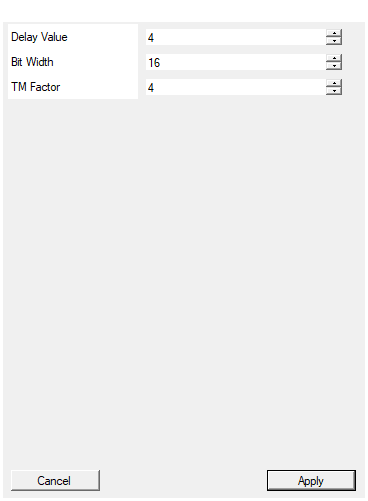
Set the delay in clock cycles introduced by the delay line
Number of clock cycles to delay all TM phases. Range: 1 – 1024 clock cycles.
This value applies identically to all TM phases and is fixed at compile time.
Total flip-flop usage = DelayValue × BusWidth × TMFactor.
Default: 4
Range: 1 – 1024
Set the size in bits of the signal to be delayed (per phase)
Bit width per TM phase (not total bus width). Range: 1 – 1024 bits.
The actual input/output width is BusWidth × TMFactor.
Default: 16
Range: 1 – 1024
Time Multiplexing factor (number of phases)
Time-multiplexing factor (number of parallel phases). Allowed values: 2, 4, 8, 16, 32 (up to 32).
Higher values increase throughput proportionally but multiply resource usage. Each TM phase uses its own delay line instance.
Default: 4
Range: 2 – 32
Functional description
The component instantiates the same fixed delay logic for each TM phase, processing all phases in parallel. The TM Factor determines how many independent delay lines are created within the component.
TM implementation
- Parallel processing: All TM phases delayed simultaneously
- Same delay: All phases use identical Delay Value
- Resource usage:
Bit Width × Delay Value × TM Factorflip-flops - Latency: Exactly $D$ clock cycles (same for all TM phases)
The input bus width is Bit Width × TM Factor, with each TM phase occupying
a contiguous slice of the input vector.
Timing
All TM phases have identical latency equal to the Delay Value:
| Property | Latency (clock cycles) |
|---|---|
| Fixed Delay TM | D |
where $D$ is the configured delay value (1-1024 clock cycles).
Typical use cases
- Multi-channel delay matching: Delaying multiple parallel ADC channels by the same amount
- TM pipeline balancing: Equalizing latencies in time-multiplexed signal paths
- Parallel synchronization: Aligning multiple TM data streams for coincidence logic
Design considerations
Resource usage multiplier
The TM version uses $\text{TM Factor}$ times more resources than the non-TM version:
- TM Factor = 4, Bit Width = 16, Delay = 10: 640 flip-flops
- TM Factor = 8, Bit Width = 16, Delay = 10: 1280 flip-flops
For large TM factors and delays, consider using the Variable Delay TM block which uses block RAM instead of registers.
Waveform example
Example with TM Factor = 4, Delay Value = 2, Bit Width = 4. Shows 4 parallel phases delayed by 2 clock cycles.
Note: The entire TM vector is delayed by 2 cycles. Each hex value represents one TM phase.