Time Multiplexing on VX2751 / DT2751 Devices
This document provides an overview of Time Multiplexing (TM) techniques for the VX2751 and DT2751 digitizers. It explains the challenges posed by the high-speed data stream generated by these devices and introduces two approaches to address them: using TM blocks for parallel processing or employing a TM Demultiplexer to adapt the data for standard blocks. The guide highlights the benefits and use cases of each method, enabling users to design efficient and reliable FPGA-based systems.
The VX2751 and DT2751 digitizers feature fast analog sampling at 1 GS/s, which enables high-resolution waveform acquisition suitable for fast detector signals.
However the FPGA embedded in these devices operates at 125 MHz, meaning it runs one clock cycle every 8 ns.
This results in a fundamental architectural implication:
For every FPGA clock cycle, 8 ADC samples arrive simultaneously.
Traditional firmware blocks in Sci-Compiler are designed to process 1 sample per cycle.
If you try to use these standard blocks directly with a 2751 digitizer, you risk losing data or misaligning signals, because the incoming data stream is 8 times faster than the logic can handle sequentially.
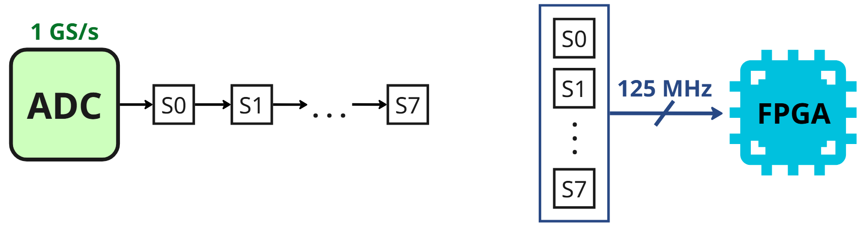
⚠️ Note: The Analog IN pins are the ADC outputs of the 2751 Digitizer. It is not possible to connect the Analog IN directly to a Sci Compiler standard block.
To address this, Sci-Compiler provides two possible and well-structured approaches, depending on the user’s needs:
Approach 1 - Use TM (Time Multiplexed) Blocks
This is the default and recommended method for working with 2751-based digitizers.
- TM blocks are special versions of standard processing blocks.
- They are designed to accept and process 8 samples simultaneously, in full parallelism, inside each FPGA clock cycle.
- Internally, TM blocks replicate the processing logic for each of the 8 samples, preserving the original block’s functionality while matching the timing structure of the digitizer.

Using TM blocks:
- Guarantees correct timing alignment
- Maintains real-time operation without data loss
- Simplifies the design by abstracting the parallel processing logic
Approach 2 - Use Standard Blocks with TM Demultiplexer
If needed, Sci-Compiler allows you to continue using standard blocks by introducing a TM Demultiplexer block at the input stage.
- The TM Demultiplexer (TM Splitter block) receives the 8-sample vector (produced each 8 ns at 1 GS/s) and breaks it down into 8 separate samples, each processed in a consecutive FPGA cycle (at 125 MHz).
- After this conversion, the data stream becomes compatible with standard single-sample blocks, and you can design the logic as in traditional lower-speed digitizers.

This approach is useful when:
- The available block in your design does not yet have a TM version.
- You prefer to work with sequential logic, processing each sample differently.