
RAM Dual Port
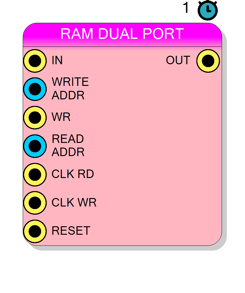
Simple dual-port RAM with independent read and write ports. Allows simultaneous read and write operations to different addresses. Write operations use WRITE_ADDR and CLK_WR; read operations use READ_ADDR and CLK_RD. Features 1 clock cycle read latency.
Introduction
This block implements a simple dual-port RAM with separate read and write ports, allowing simultaneous access to different addresses. Read and write can operate on independent clock domains.
Read latency: 1 clock cycle.
Pin Description
Properties
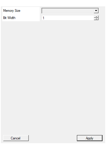
Set the amount of memory in number of words
Number of words. Allowed: 64-65536.Default: 1024
Options: 64 128 256 512 1024 2048 4096 8192 16384 32756 65536
Set the size in bits of the data
Bit width per word. Range: 1-1024.Default: 1
Range: 1 – 1024
Functional description
Dual-port RAM has independent ports:
- Write port: WRITE_ADDR, IN, WR, CLK_WR
- Read port: READ_ADDR, OUT, CLK_RD
Can read and write simultaneously to different addresses, even with different clocks.
Timing
Write: Data written to WRITE_ADDR on CLK_WR rising edge when WR=1. Read: Data from READ_ADDR available 1 cycle after CLK_RD rising edge.
Typical use cases
- Ping-pong buffers
- Cross-clock-domain data storage
- Producer-consumer queues