
SR Flip-Flop (Clocked)
Clocked Set-Reset flip-flop for synchronous bistable storage with explicit clock input. Provides synchronous set and reset control for single-bit state storage. Identical functionality to SR Flip-Flop but with visible clock input pin for explicit control. Used for control logic, flag storage, and state machines requiring direct state manipulation.
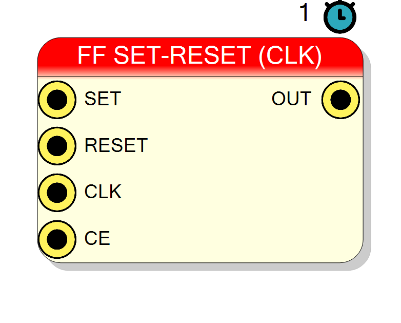
Introduction
This block implements a clocked SR (Set-Reset) flip-flop, identical to the standard SR flip-flop but with an explicit clock input pin visible on the component symbol.
The clocked SR flip-flop operates as follows:
- SET = ‘1’: Output goes to ‘1’ (set state)
- RESET = ‘1’: Output goes to ‘0’ (reset state)
- SET = ‘0’, RESET = ‘0’: Output holds its current value
- CLK pin: Explicit clock connection for synchronous operation
Key characteristics:
- Explicit clock pin: Unlike standard SR FF, clock is visible
- Direct control: No data input required
- Bistable: Two stable states (0 and 1)
- Clock enable for controlled updates
- Latency: 1 clock cycle
- Functionally identical to standard SR flip-flop
Pin Description
Clock Enable input (active high).
- CE = ‘1’: SET can control the output
- CE = ‘0’: Output holds current value (SET ignored) Note: RESET operates independently of CE. Default: ‘1’ if left unconnected.
Properties
Functional description
A clocked SR flip-flop is identical to the standard SR flip-flop in functionality, but exposes the clock input as a visible pin on the component. This allows for explicit clock domain control in designs where clock visibility is important.
Truth table
| CLK | SET | RESET | CE | Behavior |
|---|---|---|---|---|
| ↑ | X | 1 | X | OUT = ‘0’ (reset) |
| ↑ | 1 | 0 | 1 | OUT = ‘1’ (set) |
| ↑ | 0 | 0 | 1 | OUT = OUT(previous) |
| ↑ | 0 | 0 | 0 | OUT = OUT(previous) |
| ↑ | 1 | 1 | X | Undefined (avoid!) |
Note: RESET has priority over SET. Changes occur on rising clock edges (↑).
Clocked vs Standard SR Flip-Flop
Clocked SR Flip-Flop (this component):
- Explicit CLK pin visible on symbol
- Allows manual clock domain connection
- Useful when clock visibility is required
- Identical internal functionality
Standard SR Flip-Flop:
- Clock pin auto-connects to global clock
- Clock not visible on symbol
- Simpler schematic appearance
- Same internal behavior
Set operation
When SET = ‘1’ and RESET = ‘0’ and CE = ‘1’:
- Output is set to ‘1’ on the next rising clock edge
- Remains ‘1’ until RESET is asserted
Reset operation
When RESET = ‘1’:
- Output is reset to ‘0’ on the next rising clock edge
- RESET has priority over SET
- Remains ‘0’ until SET is asserted (with RESET = ‘0’)
Hold operation
When SET = ‘0’ and RESET = ‘0’:
- Output maintains its current state
- This is the memory function of the flip-flop
Clock enable
The CE input gates the SET operation:
- CE = ‘1’: SET can change the output state
- CE = ‘0’: Output holds current value
Note: RESET operates independently of CE (has priority).
Timing
| Property | Latency (clock cycles) |
|---|---|
| SR Flip-Flop (Clocked) | 1 |
State changes occur one clock cycle after SET or RESET is asserted.
Typical use cases
- Multi-clock designs: Explicit clock domain specification
- Clock gating: Manual clock control for power management
- Testbenches: Direct clock injection for verification
- Clock domain crossing: Visible clock for CDC analysis
- Debug: Explicit clock visibility for timing analysis
- All use cases of standard SR flip-flop, plus clock visibility requirements
Design considerations
- Clock connection: Must explicitly connect CLK pin (no auto-connection)
- Clock domain: Useful for designs with multiple clock domains
- Same functionality: Behaves identically to standard SR FF
- Forbidden state: Avoid SET=RESET=1 simultaneously
- Reset priority: RESET overrides SET in this implementation
Waveform example
Example showing clocked operation:
Operation is synchronized to explicit CLK input (rising edges).