
FIFO [TM]
Time-multiplexed FIFO buffer for TM data streams. Processes multiple TM phases through a shared FIFO. Xilinx FPGA implementation with independent read/write clocks and status flags.
Introduction
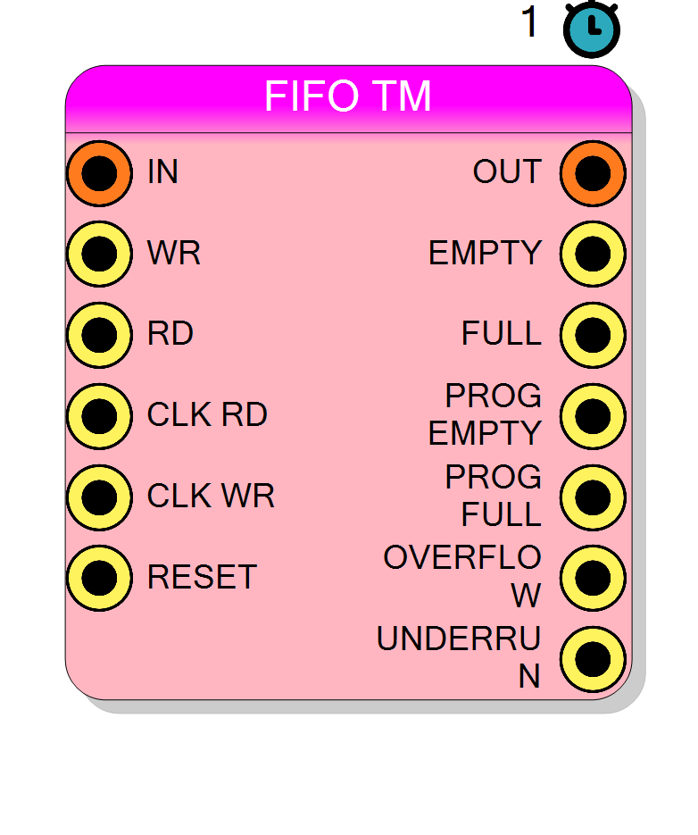
This block implements a time-multiplexed FIFO that buffers TM data streams. All TM phases are processed through the same FIFO logic.
Pin Description
Properties
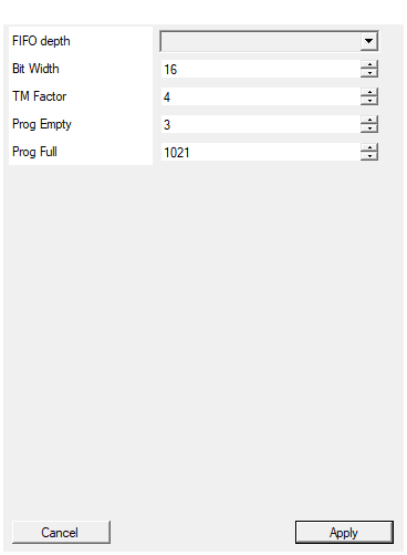
Set the amount of memory in number of words
FIFO depth. Allowed: 64-65536.Default: 1024
Options: 64 128 256 512 1024 2048 4096 8192 16384 32756 65536
Set the size in bits of the data (per phase)
Bit width per TM phase (not total).Default: 16
Range: 1 – 1024
Time Multiplexing factor (number of phases)
TM factor. Total width = BusWidth × TMFactor.Default: 4
Range: 2 – 32
Set PROG_EMPTY threshold in word. MUST BE BETWEEN 3 AND FIFO SIZE -3!
Default: 3
Range: 3 – 65535
Set PROG_FULL threshold in word. MUST BE AT MAXIMUM FIFO SIZE - 3!
Default: 1021
Range: 1 – 65535
Functional description
TM FIFO operates similarly to standard FIFO but handles TM-wide data vectors. Each FIFO entry stores an entire TM vector (all phases).
Refer to standard FIFO documentation for operational details.