
RF CIC Decimator (fixed rate)
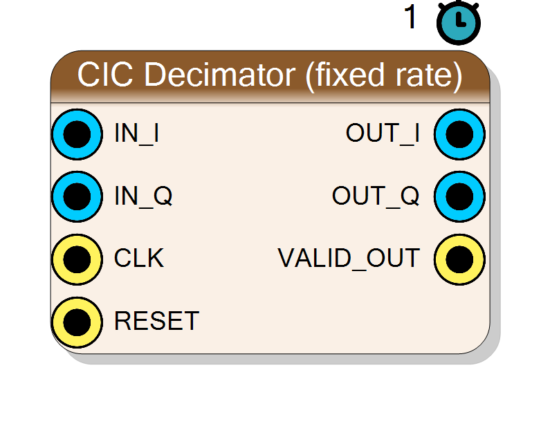
Cascaded-Integrator-Comb (CIC) decimator for a complex I/Q baseband stream. Multiplier-free anti-alias filter + down-sampler by a fixed ratio R baked into the netlist at synthesis time. Typical use: the first, highest-rate stage of a Digital Down-Converter (DDC) chain, right after the mixer, to drop the sample rate cheaply before a sharper FIR.
Introduction
The CIC Decimator (fixed rate) reduces the sample rate of a complex baseband stream by an integer factor R using a Hogenauer cascaded-integrator-comb structure. It contains no multipliers: only adders, subtractors and registers, which makes it by far the cheapest way to decimate by a large factor on an FPGA.
The datapath is three sections in series (I and Q are processed independently with identical structure):
x[n] ─► [ N integrators @ Fs_in ] ─► ( ↓R ) ─► [ N combs @ Fs_in/R ] ─► y[m]
1/(1 - z^-1) each (1 - z^-1(RM)) each
- N integrators run at the input rate
Fs_in. Each is a running accumulatorH_I(z) = 1 / (1 - z^-1). - A rate divider passes one sample every
Rclocks (↓R). - N comb stages run at the output rate
Fs_in / R. Each is a differencerH_C(z) = 1 - z^-(R*M)(referred to the input rate), i.e.1 - z^-Mat the low rate, where M is the differential delay.
The overall transfer function referred to the input rate is the classic CIC “moving-average” response:
H(z) = [ (1 - z^-(R*M)) / (1 - z^-1) ]^N
which in the frequency domain is a raised sinc:
|H(f)| = | sin(pi * R * M * f/Fs_in) / sin(pi * f/Fs_in) |^N
For a run-time programmable rate see Component_CICDecimatorProgrammable
(cic_decim_prog). For a version that also flattens the passband droop
see Component_CICCompDecim (cic_comp_decim).
Pin Description
Fs_in. Signed,
Input Bit Width bits.
Fs_in. Signed,
Input Bit Width bits. Tie to zero to decimate a purely real
signal.
Fs_in.
Default: Acquisition clock.
(R*M)^N; valid only when
VALID_OUT is high, otherwise holds the previous value.
OUT_I.
R clocks on
the cycle where OUT_I/OUT_Q carry a fresh decimated sample.
Properties
Bit width of each I/Q input sample (signed).
Bit width of each signed I / Q input sample. Range 4 to 32, default 16. Changing it triggers a redesign (re-synthesis of the HLS core).Default: 16
Options: 4 5 6 7 8 9 10 11 12 13 14 15 16 17 18 19 20 21 22 23 24 25 26 27 28 29 30 31 32
Filter order N (both integrator and comb chains). Higher N sharpens the anti-alias response but grows the accumulator width by log2(R*M) bits per stage.
Number of integrator/comb stages N (the CIC order). Higher N gives deeper alias rejection at the stop-band nulls and a sharper roll-off, but grows the accumulator width byceil(log2(R*M)) bits per stage and
increases the passband droop. Choices 1..6, default 3.
Default: 3
Options: 1 2 3 4 5 6
Down-sampling ratio. Output rate = input rate / R.
Decimation factor R (Fs_out = Fs_in / R). Baked into the netlist
as a constant. Choices 2, 4, 8, 16, 32, 64, 128, 256, default
8.
Default: 8
Options: 2 4 8 16 32 64 128 256
Differential delay of each comb stage (usually 1).
Comb differential delay M (in output-rate samples). Almost always 1;M=2 widens the stop-band notches (useful when the alias bands
are wide) at the cost of one extra bit of growth per stage. Choices
1, 2, default 1.
Default: 1
Options: 1 2
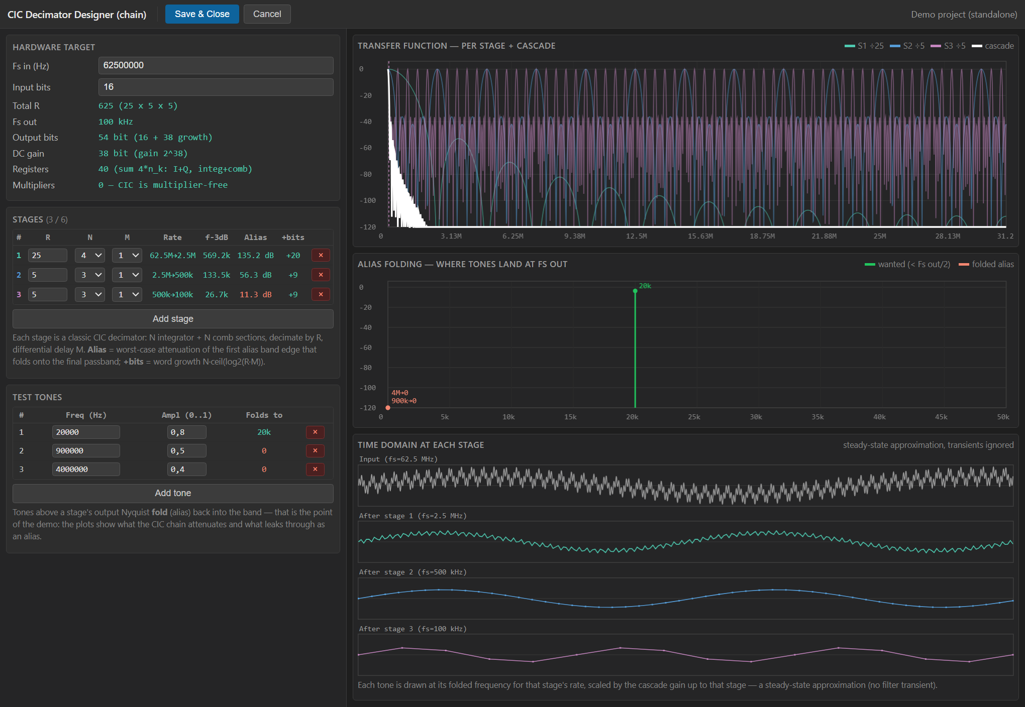
The chain design (stages + test tones), produced by the CIC Decimator Designer.
Usage
Why a CIC (and its limitations)
A CIC is a moving-average filter implemented recursively, so its cost is
independent of R. That makes it ideal for the first decimation stage where
the rate is highest. The price is a non-flat passband: the sinc^N
shape droops toward the band edge, and its stop-band nulls (located at
multiples of Fs_out) are only a few tens of dB deep for small N. A CIC
is therefore almost always followed by a compensation / channel-select
FIR that runs at the now-lower output rate.
Passband droop
Referred to the output Nyquist, the droop at a normalised output
frequency f_o = f/(Fs_out/2) is approximately
droop(dB) ~= 20*N * log10( sinc(f_o / (2R)) / sinc(1/(2R)) ) (small)
worst case at band edge ~= -3.92 * N dB (M=1, large R)
So a 3-stage CIC loses roughly 12 dB at the output band edge if you
use the full output band. Keep the useful signal well inside the band
(e.g. below 0.6-0.8 of Fs_out/2) or add a compensator.
Bit growth and accumulator width
Each integrator has unbounded DC gain, so the internal word must grow to avoid overflow. The exact register growth of a CIC is
GROWTH = N * ceil(log2(R * M))
OUT_SIZE = INPUT_SIZE + GROWTH
DC gain = (R * M)^N
The plugin sizes every integrator, comb and the output port to
OUT_SIZE bits, so the datapath is bit-true and never overflows for
full-scale input (this is the standard Hogenauer pruning-free width). The
OUT_I / OUT_Q ports carry the full un-normalised result: the DC
gain (R*M)^N is not divided out. Right-shift downstream by
log2((R*M)^N) (or use cic_comp_decim, which normalises DC gain to
unity) if you need unity-gain samples.
Worked example (defaults N=3, R=8, M=1, InputSize=16):
GROWTH = 3 * ceil(log2(8)) = 3 * 3 = 9 bits
OUT_SIZE = 16 + 9 = 25 bits
DC gain = 8^3 = 512 (= 2^9)
VALID_OUT strobe timing
The block accepts one input sample pair per clock and produces a new
output sample only once every R clocks. VALID_OUT is a one-clock-wide
strobe that marks the clock on which OUT_I/OUT_Q hold a fresh
decimated sample; between strobes the output ports simply hold their
previous value. Downstream blocks must qualify their capture with
VALID_OUT (treat it as the data-valid for the reduced-rate stream).
CLK _|‾|_|‾|_|‾|_|‾|_|‾|_ ... (R clocks) ... _|‾|_
VALID_OUT __|‾|________________ ... ...__|‾|_
^ new sample here ^ next
Timing, interface and reset
#pragma HLS PIPELINE II=1: the integrator chain runs every clock, so the block sustains one input sample pair per clock with no back-pressure.- All data ports use the
ap_noneinterface (no ready/valid handshake);RATEis tied to an internal compile-time constant (no top-level pin). RESETis the HLS synchronous reset (ap_rst): it clears the integrator accumulators, the comb delay lines, the rate-divider counter and the held output registers to zero.
Typical applications
- DDC front end :
Mixer -> cic_decim -> FIR. The CIC does the bulk rate reduction cheaply; the FIR restores a flat passband and sharp channel selectivity at the low rate. - Cheap large-factor decimation where a small passband droop is acceptable (e.g. power/energy detection, envelope tracking).
- Anti-alias + rate reduction ahead of a DMA/FIFO to cut the data rate written to memory.
Resources & Timing
-
Latency: Symbol/scheduling latency 1 clock; the first valid decimated sample appears after the rate divider fills (up to R input clocks plus the CIC group delay of ~NRM/2 input samples).
-
Throughput: 1 input sample pair per clock (II=1); one valid output sample every R clocks, flagged by VALID_OUT.
Implemented with Vitis HLS. Multiplier-free: 2N integrator adders + 2N
comb subtractors (I and Q), all OUT_SIZE = InputSize + N*ceil(log2(R*M))
bits wide, plus one rate-divider counter. Cost is independent of R, which
is what makes the CIC the cheapest large-factor decimator. Output carries
the full (R*M)^N DC gain - shift down or follow with cic_comp_decim
for a unity-gain, flat passband.