
RF CIC Decimator (programmable rate)
Cascaded-Integrator-Comb (CIC) decimator for a complex I/Q baseband stream whose decimation factor R is a run-time input pin (RATE) rather than a compile-time constant. The accumulator is sized for a worst-case MaxRate so the fabric can retune the down-sampling ratio on the fly - ideal for a software-defined DDC whose output rate must track a selected channel bandwidth.
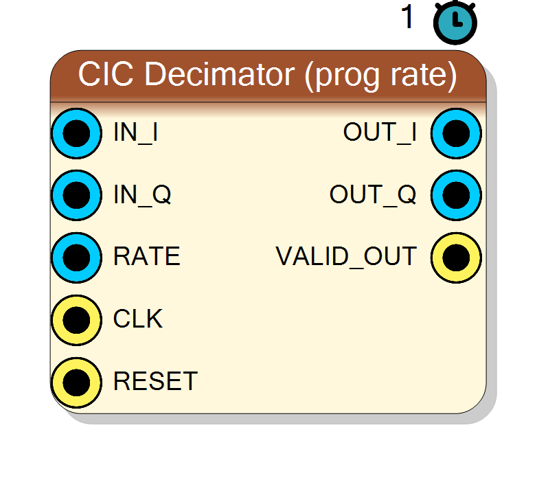
Introduction
The CIC Decimator (programmable rate) is the same Hogenauer
cascaded-integrator-comb core as Component_CICDecimator (it even
shares the identical HLS source, cic_decim.cpp, and top function
cic_decim), but the decimation ratio R is driven by a top-level
RATE input bus instead of being baked in. The fabric can change R at
any time; the change takes effect at the next rate-divider rollover.
x[n] ─► [ N integrators @ Fs_in ] ─► ( ↓R ) ─► [ N combs @ Fs_in/R ] ─► y[m]
▲
RATE pin (1..MaxRate)
The transfer function, sinc^N magnitude response and multiplier-free structure are exactly as in the fixed-rate block:
H(z) = [ (1 - z^-(R*M)) / (1 - z^-1) ]^N
|H(f)| = | sin(pi*R*M*f/Fs_in) / sin(pi*f/Fs_in) |^N
Because R is no longer known at synthesis time, the datapath must be sized for the largest rate you intend to use (the MaxRate property). This makes the accumulators wider (and the output port wider) than a fixed-rate block of the same nominal R.
See Component_CICDecimator (cic_decim) for the fixed-rate version and
the full CIC theory; this page focuses on the run-time-rate specifics.
Pin Description
Fs_in. Signed,
Input Bit Width bits.
Fs_in. Signed,
Input Bit Width bits. Tie to zero for a real-only signal.
2 .. MaxRate; a change takes effect at the next rate-divider
rollover.
Fs_in.
Default: Acquisition clock.
(R*M)^N DC gain;
valid only when VALID_OUT is high.
OUT_I.
R clocks
(with the live R) on the cycle where OUT_I/OUT_Q carry a fresh
decimated sample.
Properties
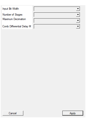
Bit width of each I/Q input sample (signed).
Bit width of each signed I / Q input sample. Range 4 to 32, default 16. Redesign on change.Default: 16
Options: 4 5 6 7 8 9 10 11 12 13 14 15 16 17 18 19 20 21 22 23 24 25 26 27 28 29 30 31 32
Filter order N.
Number of integrator/comb stages N (CIC order). Choices 1..6, default 3. Higher N deepens alias rejection but addsceil(log2(MaxRate*M)) bits of growth per stage and more passband
droop. Redesign on change.
Default: 3
Options: 1 2 3 4 5 6
Upper bound on R. Determines the accumulator width (INPUT_SIZE + Nceil(log2(MaxRateM)) bits) and the RATE bus width (ceil(log2(MaxRate))+1).
Upper bound on the run-time decimation factor R. Sizes the accumulator width (InputSize + N*ceil(log2(MaxRate*M)) bits) and the RATE bus
width (ceil(log2(MaxRate)) + 1 bits). Pick the smallest MaxRate that
covers your range to save logic. Choices 4, 8, 16, 32, 64, 128, 256,
512, default 64. Redesign on change.
Default: 64
Options: 4 8 16 32 64 128 256 512
Differential delay (usually 1).
Comb differential delay M (output-rate samples). Almost always 1;M=2 widens the stop-band notches. Choices 1, 2, default
1.
Default: 1
Options: 1 2
Usage
The RATE pin
RATE is an unsigned bus that carries the current decimation factor. Its
width is
RATE_SIZE = ceil(log2(MaxRate)) + 1 bits
The extra bit lets the value equal MaxRate itself (the rate-divider
counter counts 0 .. R-1 and compares against R). Drive RATE with any
value in 2 .. MaxRate; the block then produces one valid output every R
input clocks. A value of 0 or 1 disables decimation-by-more-than-one
and is not a useful configuration.
Worked example (default MaxRate = 64):
RATE_SIZE = ceil(log2(64)) + 1 = 6 + 1 = 7 bits (holds 0..64)
Changing RATE on the fly is glitch-safe in the sense that no sample is
corrupted, but the output rate changes at the next counter rollover, and
the CIC’s internal state (integrators/combs) reflects the previous rate
for a few output samples - allow the filter to settle after a rate change.
Bit growth is set by MaxRate, not the live rate
The accumulator width must survive the worst-case DC gain, so it is sized
from MaxRate, independent of the value you actually drive on RATE:
GROWTH = N * ceil(log2(MaxRate * M))
OUT_SIZE = INPUT_SIZE + GROWTH
DC gain = (R * M)^N (with the LIVE R, at run time)
Worked example (defaults N=3, MaxRate=64, M=1, InputSize=16):
GROWTH = 3 * ceil(log2(64)) = 3 * 6 = 18 bits
OUT_SIZE = 16 + 18 = 34 bits
RATE_SIZE = 7 bits
Note the DC gain on OUT_I/OUT_Q is (R*M)^N with the live R, so
it changes when you change the rate. Downstream normalisation (or an AGC)
must account for this if R is varied.
VALID_OUT strobe timing
Identical to the fixed-rate block: one input pair per clock in, and
VALID_OUT pulses high for one clock every R clocks marking a fresh
decimated sample on OUT_I/OUT_Q; the ports hold between strobes.
CLK _|‾|_|‾|_ ... (R clocks) ... _|‾|_
VALID_OUT __|‾|____ ... ...__|‾|_
Timing, interface and reset
#pragma HLS PIPELINE II=1: one input sample pair per clock.RATEuses theap_stableHLS interface (treated as slowly varying); all other ports useap_none.RESET(ap_rst) clears integrators, comb delay lines, the rate counter and the output holding registers.
Typical applications
- Software-defined DDC whose decimation follows a host-selected channel bandwidth without re-synthesising the bitstream.
- Multi-mode receivers that switch output rate between operating modes.
- Sweep / survey instruments that trade bandwidth for SNR at run time.
Resources & Timing
-
Latency: Symbol/scheduling latency 1 clock; first valid decimated sample after the rate divider fills (up to R input clocks) plus the CIC group delay of ~NRM/2 input samples. Allow additional settling after a run-time rate change.
-
Throughput: 1 input sample pair per clock (II=1); one valid output sample every R input clocks (live R), flagged by VALID_OUT.
Same HLS core as the fixed-rate cic_decim (top function cic_decim),
with RATE promoted to a top-level ap_stable port. Datapath sized for
MaxRate, so it is wider/costlier than a fixed-rate block of equal nominal
R - use the smallest MaxRate you need. Multiplier-free: 2N integrator
adders + 2N comb subtractors + one comparator/counter. Output carries
the live (R*M)^N DC gain; normalise downstream (or use
cic_comp_decim).