
CFD (Constant Fraction Discriminator)
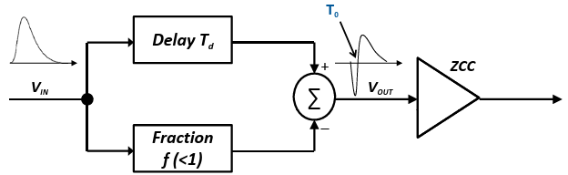
Digital Constant Fraction Discriminator for a signal with one sample per clock. It subtracts a fraction of the live signal from a delayed copy and triggers on the zero crossing of the result, so the trigger time does not depend on the pulse amplitude. Optional linear interpolation gives the crossing position with a resolution of 1/2048 of a sample. It is the single-sample twin of CFD - TM.
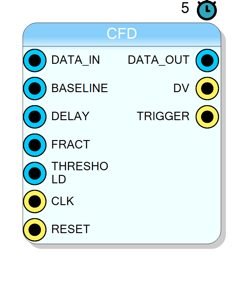
Introduction
The CFD generates a timing marker that does not walk with the pulse amplitude. It computes
$$ V_{\mathrm{out}}[n] = \bigl(x[n-D] - B\bigr) - f \cdot \bigl(x[n] - B\bigr) $$
where $D$ is the delay in samples (DELAY), $f$ the fraction (FRACT, $0 \le f < 1$) and $B$ the BASELINE. For a positive pulse $V_{\mathrm{out}}$ first dips (the live signal rises before the delayed one) and then crosses zero: the block arms when $V_{\mathrm{out}} < -\text{THRESHOLD}$ and fires TRIGGER on the first sample with $V_{\mathrm{out}} \ge 0$ after arming.
If the pulse is a scaled shape, $x[n] - B = A \cdot s[n]$, then $V_{\mathrm{out}}[n] = A,\bigl(s[n-D] - f,s[n]\bigr)$: the amplitude $A$ multiplies everything and the zero crossing does not move. A pulse twice as big triggers on the same sample, with the same interpolated position.
Use CFD when the signal has one sample per clock; for time-multiplexed digitizers (2-16 samples per clock word) use CFD - TM, which implements the same algorithm.
Pin Description
Properties
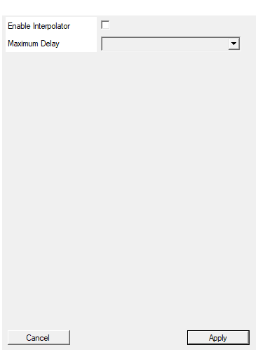
Linear interpolation of the zero crossing (dT INTERPOLED / DV_DT outputs). Adds a divider: latency 54 clocks instead of 5.
Adds the linear interpolation of the zero crossing and the dT INTERPOLED / DV_DT outputs. Latency 54 clocks instead of 5 at 125 MHz, about 4400 FF and 3400 LUT more.Default: False
Depth of the delay memory in samples. The largest usable DELAY is this value minus 1; larger DELAY values are clamped.
Depth of the delay memory in samples (64 to 16384). The largest usable DELAY is this value minus 1. 1024 fits one BRAM18.Default: 1024
Options: 64 128 256 512 1024 2048 4096 8192 16384
Functional description
| Stage | Function |
|---|---|
| Delay line | circular memory of Maximum Delay samples, read at $n - D$ |
| Baseline | $x - B$ on both the live and the delayed sample (16-bit two’s complement) |
| CFD sum | $V_{\mathrm{out}} = (x_{del} - B) - f,(x - B)$, exact (32-bit + 16 fractional bits) |
| Arm / fire | arm below $-\text{THRESHOLD}$, fire on the first $V_{\mathrm{out}} \ge 0$ |
| Interpolator | optional: position of the zero crossing between two samples |
Arming and triggering
- The block is armed on a sample where $V_{\mathrm{out}} < -\text{THRESHOLD}$.
- Once armed, TRIGGER is high for one clock on the first sample with $V_{\mathrm{out}} \ge 0$; this disarms the block.
- A crossing without a previous arming is ignored: THRESHOLD is the noise rejection. A pulse too small to bring $V_{\mathrm{out}}$ below $-\text{THRESHOLD}$ never triggers.
Interpolated position
With Enable Interpolator the block also computes where, between the previous sample ($V_p < 0$) and the trigger sample ($V_c \ge 0$), the straight line crosses zero:
$$ \mathrm{dT} = \frac{-V_p}{V_c - V_p} \in (0, 1] $$
dT INTERPOLED carries it with 11 fractional bits (value / 2048), the
same format as CFD - TM (ap_fixed<16,5>). The crossing time is
$$ t_{\mathrm{cross}} = n_{\mathrm{TRIGGER}} - 1 + \frac{\mathrm{dT}}{2048} $$
i.e. dT is measured from the sample before the trigger: a value of 1462 means the crossing lies 0.714 samples after that sample, 0.286 samples before the trigger sample. DV_DT pulses with the new value; dT INTERPOLED holds it until the next trigger. Without the interpolator these two pins are not on the symbol.
DATA_OUT and DV
DATA_OUT is $V_{\mathrm{out}}$ rounded down to an integer (16-bit two’s complement), useful to look at the CFD signal while tuning DELAY and FRACT. DV is high on every clock once the pipeline is full.
Latency
All outputs (DATA_OUT, TRIGGER, dT INTERPOLED) leave the block on the same clock, a fixed number of clocks after the input sample:
| Clock | Without interpolator | With interpolator |
|---|---|---|
| 125 MHz | 5 clocks | 54 clocks |
| 250 MHz | 9 clocks | 58 clocks (divider estimated at 213 MHz) |
Values measured on the Vitis HLS 2020.2 output; the symbol reports the 125 MHz figures. When TRIGGER is used to time other signals, delay those by the same amount. With the interpolator above ~200 MHz the divider may not meet timing.
Start-up and DELAY changes
The delay memory is empty (0) after FPGA configuration. During the first DELAY clocks the delayed sample is 0 instead of the signal: with a non-zero BASELINE this gives a large negative $V_{\mathrm{out}}$ and one spurious TRIGGER when the memory fills. The same mechanism applies after changing DELAY at run time: for DELAY samples the comparison uses older data. Ignore triggers in that window if it matters.
Timing diagram
Delay 3, f = 0.5, threshold 100, baseline 1000, pulse of amplitude 1000 starting at sample 0 (4-sample linear rise, then x0.8 decay). Values of DATA_OUT as computed by the block; outputs shown without the pipeline latency:
DATA_OUT drops below -100 at sample 1 (armed) and becomes positive at sample 5: TRIGGER. dT = 250 / (100 + 250) = 0.714 -> 1462. The same pulse at amplitude 2000 gives exactly the same TRIGGER sample and dT.
The Test Timing window (right click on the block) shows this pulse, the same shape at double amplitude, and a small pulse below threshold.
Choosing the parameters
- DELAY: about the rise time of the pulse, so the crossing falls on the leading edge. Range 0 to Maximum Delay - 1 (larger values are clamped). DELAY = 0 compares the signal with itself and never triggers on positive pulses.
- FRACT: unsigned Q0.16, 0x0000 = 0, 0x8000 = 0.5, 0xFFFF = 0.99998. Typical 0.2-0.5: the trigger happens where the delayed pulse reaches FRACT of the live one.
- THRESHOLD: in ADC counts, compared with $-V_{\mathrm{out}}$. Above the noise of $V_{\mathrm{out}}$, below the dip of the smallest pulse to keep.
- BASELINE: the signal level with no pulse. $x - B$ must fit 16 bits signed ($\pm 32767$); the block is designed for positive pulses (for negative pulses invert the signal first).
Resources
Without the interpolator: 1 BRAM18 (Maximum Delay = 1024), 1 DSP, a few hundred FF/LUT. The interpolator adds a 45/34-bit divider of about 4400 FF and 3400 LUT.
Resources & Timing
-
Latency: 5 clocks (54 with the interpolator) at 125 MHz; 9 / 58 at 250 MHz
-
Throughput: 1 sample per clock (II=1)
HLS core Resources/Code/cfd.cpp, exact integer arithmetic. 1 BRAM18 per 1024 samples of delay, 1 DSP; the optional divider adds ~4400 FF and ~3400 LUT.