
Wire Split
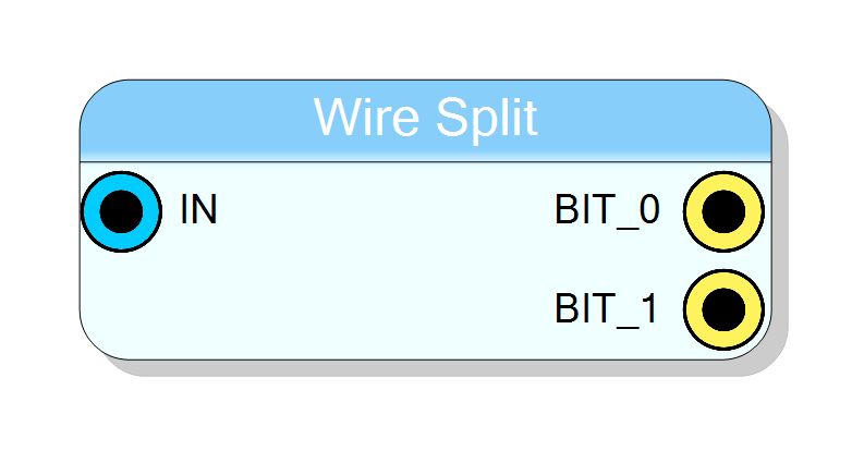
Bit splitting operation. Splits a single input vector into multiple single-bit output vectors, one for each bit of the input. Configurable bit ordering (LSB-first or MSB-first). Pure combinational logic (zero latency). Essential for bit field unpacking and individual bit access.
Introduction
This block performs bit splitting on standard (non-TM) data streams. It receives a single input vector and splits it into N individual single-bit outputs, where N is the width of the input vector.
The operation is purely combinational with zero clock latency.
Output bit ordering is configurable:
- BIT 0 is MSB: First output is the MSB of input
- BIT 0 is LSB: First output is the LSB of input
Pin Description
Properties
Set the bits of the input
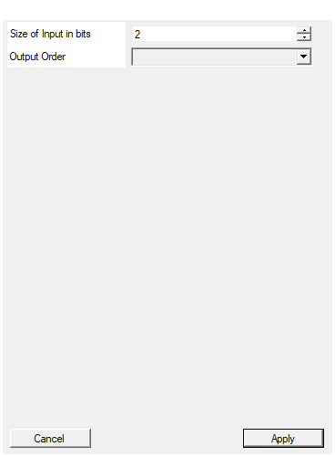
Size of input vector in bits. Range: 2 – 16384. Determines the number of output bits (one output per input bit).Default: 2
Range: 2 – 16384
Select if output BIT 0 is LSB or MSB on input vector
Bit ordering mode:
BIT 0 is MSB→ First output is input MSBBIT 0 is LSB→ First output is input LSB
Default: BIT 0 is MSB
Options: BIT 0 is MSB BIT 0 is LSB
Functional description
Wire Split extracts each bit from the input vector into separate output pins.
Bit ordering modes
-
BIT 0 is MSB:
- OUT_0 = input MSB (leftmost bit)
- OUT_N-1 = input LSB (rightmost bit)
- Example: IN=
ABCD(4 bits) → OUT_0=A, OUT_1=B, OUT_2=C, OUT_3=D
-
BIT 0 is LSB:
- OUT_0 = input LSB (rightmost bit)
- OUT_N-1 = input MSB (leftmost bit)
- Example: IN=
ABCD(4 bits) → OUT_0=D, OUT_1=C, OUT_2=B, OUT_3=A
Example
Given an 8-bit input 10110011:
- BIT 0 is MSB: OUT_0=1, OUT_1=0, OUT_2=1, …, OUT_7=1
- BIT 0 is LSB: OUT_0=1, OUT_1=1, OUT_2=0, …, OUT_7=1
Timing
Purely combinational with zero latency.
Typical use cases
- Extracting individual status flags from status registers
- Unpacking bit fields from protocol frames
- Converting parallel buses to individual signals
- Accessing individual bits for control logic