
RF AM Demod (envelope)
Envelope AM demodulator. A real passband AM signal is rectified, low-pass filtered and DC-blocked; a complex I/Q baseband signal is passed through an alpha-max-beta-min magnitude estimator and DC-blocked. Output is the recovered message. The low-pass and DC-block time constants are run-time pins.
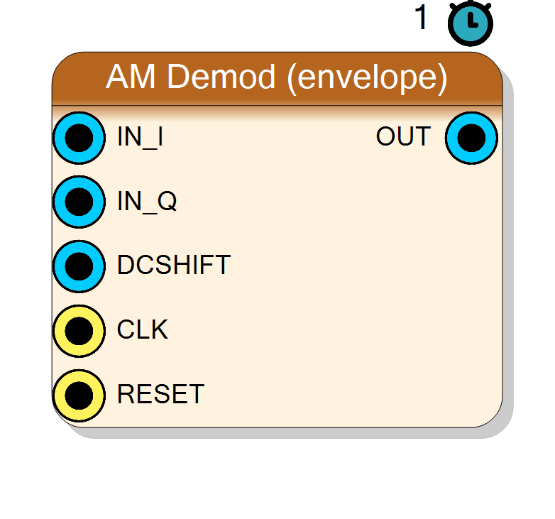
Introduction
The AM Demod (envelope) block recovers the message from an AM signal in one of two ways, chosen by the Signal Type property:
-
Real (passband AM): rectify the input, low-pass it to strip the carrier, then DC-block to remove the carrier pedestal.
rect[n] = |x[n]| lp[n] = lp[n-1] + (rect[n] - lp[n-1]) >> LPSHIFT (1-pole LPF) env[n] = lp[n] -
Complex (I/Q baseband, e.g. after a DDC or the Hilbert block): estimate the magnitude with the alpha-max-beta-min approximation, then DC-block.
env[n] = max(|I|,|Q|) + (min(|I|,|Q|) >> 1)
Both paths finish with a DC blocker whose output is the recovered message:
dc[n] = dc[n-1] + (env[n] - (dc[n-1] >> DCSHIFT))
y[n] = env[n] - (dc[n] >> DCSHIFT)
For a real passband AM signal put a DDC (mixer + decimator) or a Hilbert block in front and use the Complex path. This block uses the standard property grid (no custom designer).
Pin Description
InputSize bits.
InputSize bits.
~ 2^DCSHIFT samples). Present
in both modes. Unsigned 5 bits (0..31).
InputSize + 1 bits.
InputSize bits.
~ 2^LPSHIFT samples).
Present ONLY in Real mode. Unsigned 5 bits (0..31).
Properties
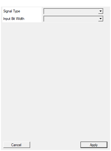
Real: passband AM (rectify+LPF). Complex: I/Q baseband (|I+jQ|).
Real: passband AM, rectify + 1-pole LPF + DC block (adds the LPSHIFT pin). Complex: I/Q baseband, alpha-max-beta-min magnitude + DC block (adds IN_I / IN_Q). Default Complex. Changing it redesigns the core (pin set changes).Default: Complex
Options: Real Complex
Input bit width.
Input bit width. Range 4 to 32, default 16.Default: 16
Options: 4 5 6 7 8 9 10 11 12 13 14 15 16 17 18 19 20 21 22 23 24 25 26 27 28 29 30 31 32
Usage
Runtime pins vs static properties
- LPSHIFT[4:0] - run-time pin, present ONLY in Real mode. The 1-pole
low-pass shift (time constant
~ 2^LPSHIFTsamples). Larger = slower / smoother carrier removal. - DCSHIFT[4:0] - run-time pin, present in BOTH modes. The DC-blocker
shift (time constant
~ 2^DCSHIFTsamples). Larger = slower DC tracking, passing lower message frequencies. - Both shift pins are
SHIFT_BITS = 5wide, so each carries 0..31. Drive them from a register or a constant. - Signal Type and Input Bit Width are the only static properties.
Rule of thumb for the time constants:
f_dc << f_message << Fs / (2*pi*2^LPSHIFT) << f_carrier
Reset requirement (config_rtl -reset state)
The low-pass and DC-blocker accumulators are static feedback registers. In
a Vitis default config_rtl -reset control build these static-derived
registers are not reset, so any X present on the input during the first
simulation cycles latches into the IIR feedback and the output stays X
forever. This block therefore injects config_rtl -reset state into its HLS
script so the accumulators start clean once RESET deasserts. (It is injected
only for this block, to avoid resetting the large static arrays - FIR delay
lines, FFT buffers - in the other shared RF blocks.)
Bit widths
IN/IN_I/IN_Q: signedInputSizebits.LPSHIFT,DCSHIFT: unsigned 5 bits.OUT: signedInputSize + 1bits.- Internal DC accumulator carries
InputSize + 2 + 31bits of headroom so the largest DCSHIFT never loses resolution.
Latency and throughput
#pragma HLS PIPELINE II=1: one output sample per clock.- All ports use the
ap_noneinterface (no ready/valid handshake). - INTERFACE pragmas are emitted before any statement so Vitis keeps
ap_ctrl_none(free-running; SciCompiler never drivesap_start).
Reset
RESET is the HLS synchronous reset (ap_rst) and, thanks to the
-reset state option above, clears the LP and DC feedback accumulators.
Typical applications
- Envelope detection of a real passband AM carrier (Real mode).
- Magnitude / envelope recovery of an I/Q baseband stream after a DDC or the Hilbert block (Complex mode).
Resources & Timing
-
Latency: 1 clock cycle (II=1)
-
Throughput: 1 sample per clock (II=1)
Implemented with Vitis HLS. No multipliers: the Real path is a rectifier
plus a shift-based 1-pole IIR; the Complex path is the alpha-max-beta-min
magnitude (compare + one shift-add). Both share a shift-based DC blocker.
The HLS unique name depends only on InputSize and Signal Type; LPSHIFT /
DCSHIFT are runtime pins and are excluded. Requires config_rtl -reset state so the IIR accumulators clear on reset.