Memory Mapped Components
Guide to memory-mapped components (MMC) in SCI-Compiler. Learn the difference between stand-alone and memory-mapped blocks, understand endpoint creation, configure address mapping, work with sub-designs containing MMC, and understand RegisterFile.json structure for SDK integration.
Introduction
SCI-Compiler components are divided into two fundamental categories based on their interaction with the host PC:
- Stand-alone components - Operate independently without PC communication
- Memory-mapped components (MMC) - Require PC communication via memory-mapped interface
Understanding this distinction is crucial for proper firmware design and SDK integration.
Stand-Alone Components
Stand-alone components perform their function entirely within the FPGA without requiring communication with the host PC.
Characteristics
- No PC interface - Operate autonomously
- Configurable parameters - Set at design time or via registers
- Pure FPGA logic - No SDK functions required
- Performance - No communication overhead
Examples
Boolean Logic:
- AND, OR, XOR, NOT gates
- Reduce operations
- Comparators
Mathematical Operations:
- Adders, Subtractors, Multipliers
- Absolute value
- Min/Max functions
Signal Processing:
- Trapezoidal filter
- Leading/Trailing edge triggers
- Baseline restorer
- Time-over-Threshold (ToT)
Timing:
- Counters
- Chronometers
- Delays
- Pulse generators
Configuration
Stand-alone components are configured via:
- Block properties - Set at design time
- Register inputs - Runtime configuration via memory-mapped registers
- Hard-coded values - Constants in the design
Memory-Mapped Components (MMC)
Memory-mapped components require bidirectional communication with the host PC for configuration and data transfer.
Characteristics
- PC interface required - Communicate via USB/Ethernet/VME
- Address-based access - Accessed via memory-mapped addressing
- SDK functions - Automatically generated C/Python libraries
- Data acquisition - Transfer large amounts of data to PC
Examples
Data Acquisition (DAQ):
- Oscilloscope - Waveform capture
- Spectrum - 1D histogram (MCA)
- 2D Histogram - Imaging spectrum
- Imaging Module - 2D pixel data
- Logic Analyzer - Digital signal capture
Data Streaming:
- List - Event-by-event data stream
- Digitizer - Continuous ADC streaming
- Custom Packet Creator - User-defined data packets
Communication Interfaces:
- I2C Master (memory-mapped mode)
- Register Read/Write blocks
Board-Specific:
- Petiroc/Citiroc Slow Control
- HV Controller
- Custom peripherals
Endpoint Creation
When you add a memory-mapped component to your design, SCI-Compiler creates an endpoint.
What is an Endpoint?
An endpoint is the combination of:
- FPGA module - VHDL implementation of the block
- SDK functions - C/Python library functions for PC interaction
- Memory mapping - Address space allocation
- RegisterFile entry - JSON descriptor for SDK
Configuration Dialog
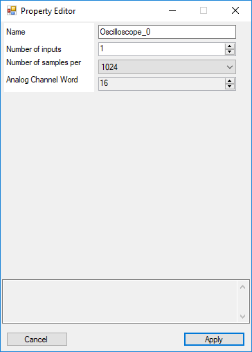
Figure 1: Oscilloscope endpoint configuration
When adding an MMC block, a configuration dialog appears with:
Endpoint Name:
- Must be unique across entire project
- Used to generate SDK function names
- Appears in block diagram
- Included in RegisterFile.json
Block-specific parameters:
- Buffer size (samples per channel)
- Number of channels
- Data width
- Trigger mode
- Other options specific to block type
SDK Function Generation
For an oscilloscope named Oscilloscope_0, SCI-Compiler generates functions:
// C API
SCILIB int OSCILLOSCOPE_Oscilloscope_0_START(void* handle);
SCILIB int OSCILLOSCOPE_Oscilloscope_0_SET_PARAMETERS(void* handle, ...);
SCILIB int OSCILLOSCOPE_Oscilloscope_0_DOWNLOAD(void* handle, void* buffer);
SCILIB int OSCILLOSCOPE_Oscilloscope_0_STOP(void* handle);
# Python API
oscilloscope_0.start()
oscilloscope_0.set_parameters(...)
oscilloscope_0.download(buffer)
oscilloscope_0.stop()
Naming convention:
<BLOCK_TYPE>_<ENDPOINT_NAME>_<FUNCTION>
Endpoint Representation in Diagram
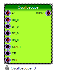
Figure 2: Endpoint block in diagram
Memory-mapped blocks are shown as:
- Standard block with inputs/outputs
- Small icon at bottom (endpoint indicator)
- Endpoint name displayed below block
The endpoint indicator distinguishes MMC from stand-alone blocks.
Memory Mapping Tab
All memory-mapped endpoints must be assigned addresses in the Memory Mapping tab.
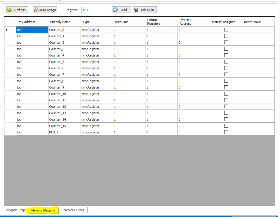
Figure 3: Memory Mapping tab showing endpoints
Accessing Memory Mapping
- Click Memory Mapping tab at bottom of IDE
- Tab lists all registers and MMC endpoints
- Initially, addresses are not assigned
Refresh List
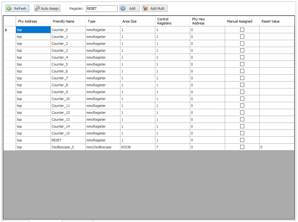
Figure 4: Refresh button to update endpoint list
Important: When adding new endpoints to diagram:
- Click Refresh button
- New endpoints appear in list
- Addresses can then be assigned
Address Assignment
Each endpoint requires a unique memory address range.
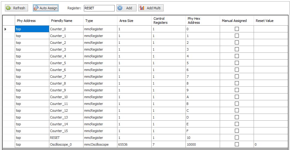
Figure 5: Address assignment with Auto Assign
Address Space Concepts
Phy Hex Address:
- Base address (starting address) of endpoint
- Entered in hexadecimal
- Must be unique (no overlaps)
Area Size:
- Memory space required by endpoint (in words)
- Automatically calculated by SCI-Compiler
- Depends on buffer size, channels, data width
Control Registers:
- Number of configuration/status registers
- Additional to data buffer area
- Used for control and status
Manual vs. Automatic Assignment
Manual Assignment:
- Check Manual Assigned checkbox
- Enter address in Phy Hex Address column
- Address is protected from Auto Assign
Automatic Assignment:
- Click Auto Assign button
- SCI-Compiler calculates optimal layout
- Ensures no overlaps
- Fills gaps efficiently
Recommendation: Use Auto Assign unless you have specific address requirements.
Address Calculation Example
For a register:
- Area Size: 1 word
- Address: 0x0000
For an oscilloscope (1024 samples, 4 channels, 16-bit):
- Area Size: 1024 × 4 = 4096 words
- Control Registers: ~10
- Total: 4106 words
- Address range: 0x1000 - 0x200A (example)
Avoiding Address Conflicts
Critical: Ensure no overlap between address spaces!
Address conflict example (BAD):
Endpoint_A: 0x0000 - 0x1000 (4096 words)
Endpoint_B: 0x0800 - 0x1800 (4096 words) ← CONFLICT at 0x0800-0x1000!
Correct layout:
Endpoint_A: 0x0000 - 0x1000 (4096 words)
Endpoint_B: 0x1000 - 0x2000 (4096 words) ← No conflict
Use Auto Assign to prevent conflicts automatically.
Sub-Designs with Memory-Mapped Components
Since SCI-Compiler 2024.1.x.x, memory-mapped components can be placed inside sub-designs, and the sub-design itself becomes a memory-mapped component.
Hierarchical MMC
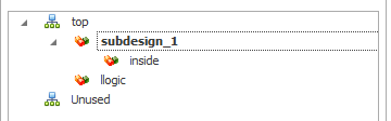
Figure 6: Sub-design containing oscilloscope and registers
A sub-design containing MMC blocks:
- Oscilloscope
- Registers
- Other MMC endpoints
Sub-Design Diagram
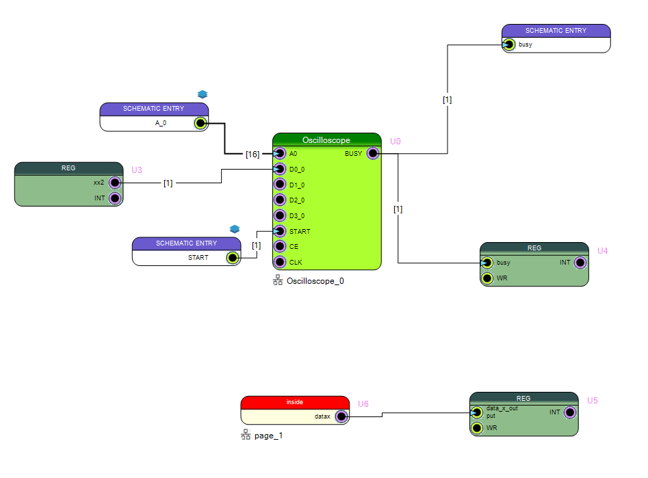
Figure 7: Internal diagram of sub-design with MMC
The sub-design has its own block diagram with memory-mapped components.
Sub-Design Memory Mapping
Each sub-design has its own Memory Mapping tab.
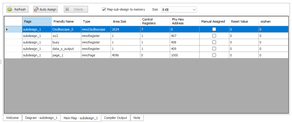
Figure 8: Sub-design Memory Mapping tab
Relative Addressing
Important: Addresses in sub-design are relative to page base address.
Full address calculation:
Full_Address = Page_Base_Address + Component_Relative_Address
Enable/Disable Memory Mapping
Map sub-design to memory checkbox:
- Checked: Sub-design is memory-mapped (occupies address space)
- Unchecked: Sub-design is stand-alone (legacy compatibility)
Default: Unchecked for backward compatibility with older projects.
Memory Space (Size):
- Total address space required by sub-design
- Automatically calculated by Auto Assign
- Can be manually reserved
Auto Assign for Sub-Designs
Click Auto Assign in sub-design Memory Mapping tab:
- Calculates all component addresses (relative)
- Determines total memory space (Size)
- Allocates space efficiently
Sub-Design as Endpoint
When inserted in parent design, sub-design appears as an MMC endpoint.
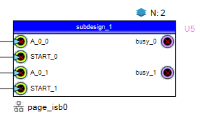
Figure 9: Sub-design shown as endpoint in parent diagram
Characteristics:
- Endpoint icon at bottom
- Sub-design name shown
- Inputs/outputs as defined
- Occupies memory address range
Parent Memory Mapping
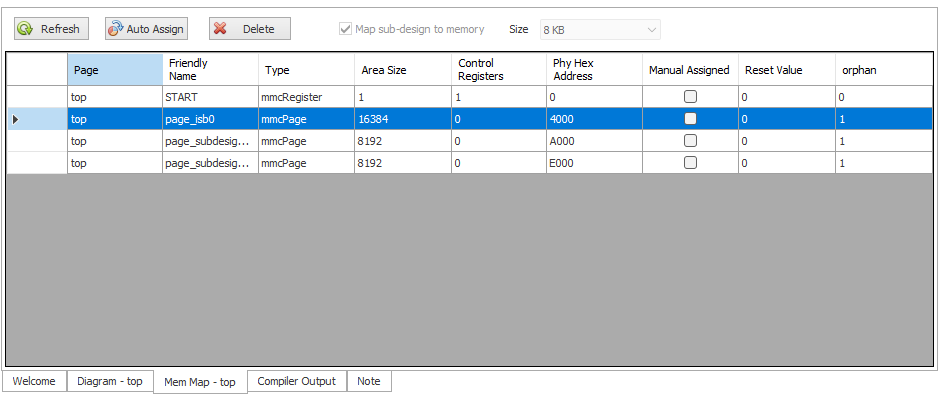
Figure 10: Sub-design in parent Memory Mapping tab
In the parent’s Memory Mapping tab, the sub-design appears as:
- Single entry with sub-design name
- Base address assignment
- Total area size (sum of all internal components)
Multi-Channel Sub-Designs
If configured as Multi-Channel device:
- Memory area = N × Single_Page_Memory
- Each instance has separate address range
- Allows replication of complex processing chains
Example:
- Single page: 8KB memory
- 4 channels configured
- Total memory: 4 × 8KB = 32KB
RegisterFile.json
SCI-Compiler generates RegisterFile.json during compilation, describing all memory-mapped components for SDK usage.
Endpoint Names in RegisterFile
For components inside sub-designs, the full name format is:
<PAGE_NAME>_<REPETITION>_<COMPONENT_NAME>
Example:
json
"Name": "page_isb0_1_Oscilloscope_0"
Where:
page_isb0- Sub-design (page) name1- Repetition index (for multi-channel)Oscilloscope_0- Component name inside sub-design
RegisterFile Structure
json
{
"Device": "DT5550",
"Magic": "593AE14D",
"Project": "my_project",
"Registers": [
{
"Name": "threshold",
"Address": 0,
"RegionSize": 1,
"Description": "Trigger threshold"
}
],
"MMCComponents": [
{
"Name": "Oscilloscope_0",
"Type": "Oscilloscope",
"Address": 4096,
"Version": "1.0.0.0",
"channels": 4,
"samples": 1024,
"Registers": [...]
},
{
"Name": "page_isb0_0_Spectrum_0",
"Type": "Spectrum",
"Address": 8192,
"bins": 8192,
"Registers": [...]
}
]
}
Working with MMC - Best Practices
Naming Conventions
Good endpoint names:
Oscilloscope_TriggerSpectrum_Energy_Ch0List_EventData- Descriptive, unique, no spaces
Bad endpoint names:
Osc1(not descriptive)My Scope(contains space)Test(too generic)
Address Planning
For simple designs:
- Use Auto Assign - it works well
For complex designs:
- Group related endpoints
- Leave gaps for future expansion
- Document address map
- Use manual assignment for critical blocks
Memory Optimization
Reduce memory usage:
- Minimize buffer sizes where possible
- Use appropriate data widths (don’t default to 32-bit)
- Share registers between channels
- Consider using List endpoint instead of Oscilloscope for events
Example optimization:
- Oscilloscope: 1024 samples × 16 channels = 16K words
- Better: 512 samples × 16 channels = 8K words (if sufficient)
Sub-Design Organization
When to use sub-designs:
- Repeating processing chains (multi-channel)
- Functional grouping (trigger system, DAQ system)
- Design modularity and reuse
- Team collaboration (separate sub-systems)
When NOT to use sub-designs:
- Simple single-channel designs
- No repeated structures
- Adds unnecessary complexity
Common Workflows
Adding First MMC Endpoint
- Drag Oscilloscope from Tools Box → Diagram
- Configuration dialog appears
- Enter endpoint name:
Oscilloscope_0 - Configure channels, samples
- Click OK
- Switch to Memory Mapping tab
- Click Refresh
- Click Auto Assign
- Addresses assigned automatically
Adding Multiple Endpoints
- Add all MMC blocks to diagram
- Configure each with unique name
- Switch to Memory Mapping tab
- Click Refresh (updates list)
- Click Auto Assign
- Verify no address conflicts (check Area Size)
Creating Hierarchical Design
- Create sub-design (Project Files → New)
- Design processing chain in sub-design
- Add MMC blocks (registers, oscilloscope, etc.)
- Switch to sub-design Memory Mapping tab
- Check Map sub-design to memory
- Click Auto Assign
- Return to main design
- Add sub-design block to main diagram
- Refresh and Auto Assign in main Memory Mapping
Fixing Address Conflicts
If compilation errors mention address conflicts:
- Open Memory Mapping tab
- Look for overlapping address ranges
- Click Auto Assign to recalculate
- Or manually adjust conflicting addresses
- Recompile
Troubleshooting
Endpoint Not Appearing in Memory Mapping
Problem: Added MMC block but not in Memory Mapping tab
Solutions:
- Click Refresh button
- Ensure block configuration completed (didn’t cancel)
- Check block has endpoint icon (memory-mapped)
- Switch to different tab and back
Address Conflict Errors
Problem: Compilation fails with address overlap errors
Solutions:
- Click Auto Assign to recalculate
- Manually check address ranges don’t overlap
- Verify Area Size + Base Address < Next Base Address
- Increase spacing between endpoints
SDK Functions Not Generated
Problem: Can’t find ENDPOINT_Name_FUNCTION in SDK
Solutions:
- Verify endpoint name is correct (case-sensitive)
- Check RegisterFile.json was generated
- Recompile project
- Ensure library folder contains SDK files
- Check for compilation errors
Sub-Design Endpoint Not Working
Problem: Sub-design doesn’t appear as endpoint
Solutions:
- Verify Map sub-design to memory is checked
- Ensure sub-design contains MMC components
- Click Refresh in parent Memory Mapping
- Run Auto Assign in sub-design first
- Synchronize sub-design (Sync button)
RegisterFile.json Missing
Problem: RegisterFile.json not created after compilation
Solutions:
- Compilation must complete successfully
- Check compiler output for errors
- File location:
ProjectFolder/library/RegisterFile.json - Ensure at least one register or MMC in design
Summary
Memory-mapped components are essential for PC-FPGA communication:
| Aspect | Details |
|---|---|
| Component types | Stand-alone vs. Memory-mapped |
| MMC examples | Oscilloscope, Spectrum, List, Registers |
| Endpoints | FPGA module + SDK functions |
| Memory Mapping | Address assignment for each endpoint |
| Sub-designs | Hierarchical MMC since v2024.1 |
| RegisterFile.json | SDK descriptor generated at compile |
| SDK functions | Auto-generated C/Python API |
Key operations:
- Add MMC block → Configure endpoint name
- Memory Mapping tab → Refresh
- Auto Assign addresses
- Compile → RegisterFile.json generated
- Use SDK functions with endpoint name
Memory-mapped components bridge FPGA processing with PC-based analysis and control!