
Position Sense Detector
Calculates the interaction position on a position-sensitive detector (e.g., He3 tube) by measuring the energy on both sides of the detector. Implements a quasi-Gaussian shaper filter for signal processing and peak detection.
Introduction
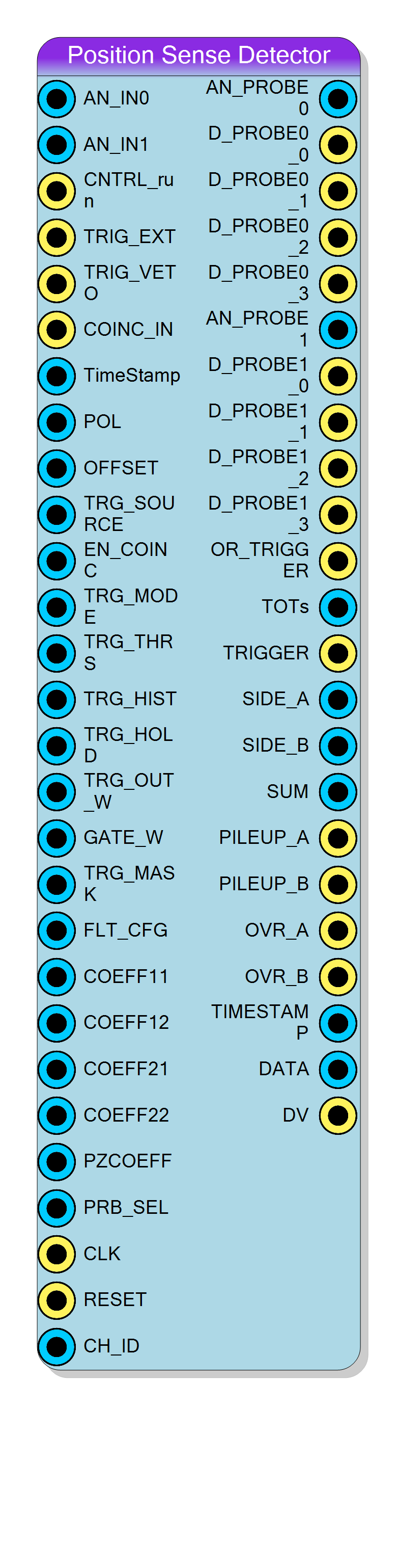
The Position Sense Detector (NI_PSA) block calculates the interaction position of a particle (e.g., a neutron) on a position-sensitive detector such as a He3 tube. It measures the energy on both sides of the detector and determines the position from the ratio between one side’s energy and the total energy sum.
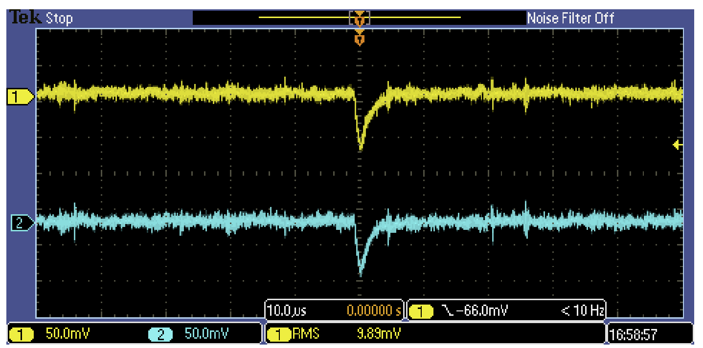
Key principle: When a particle interacts with the detector, charge is collected at both ends. The ratio of charge collected at one end to the total charge is proportional to the interaction position along the detector.
$$ \text{Position} = \frac{E_A}{E_A + E_B} $$
where $E_A$ and $E_B$ are the energies measured on side A and side B respectively.
Pin Description
Enable signal for the processing core.
- 1: Core enabled, processing active
- 0: Core disabled Default: 1.
Signal polarity selection.
- 0: Positive pulses
- 1: Negative pulses (inverts input)
Trigger datapath selection.
- 0: Use shaped (filtered) signal for trigger
- 1: Use raw input signal for trigger
Coincidence validation enable.
- 0: No validation required, events always output
- 1: Require COINC_IN HIGH during gate window
Internal trigger mode selection.
- 0: Trigger on sum of both sides (A + B)
- 1: External trigger only (internal disabled)
- 2: Trigger on OR of both sides
- 3: Trigger on AND of both sides Note: External trigger is always enabled regardless of this setting.
Channel trigger mask.
- 0: Both sides enabled
- 1: Side A masked
- 2: Side B masked
- 3: Both sides masked
Filter configuration register. Suggested starting value: 0x1F33.
- Bits 3:0 - Attenuation section 1 (0=min, F=max)
- Bits 7:4 - Attenuation section 2 (0=min, F=max)
- Bit 8 - Enable input baseline correction
- Bit 9 - Enable pole-zero compensation
- Bit 10 - Enable first Gaussian filter section
- Bit 11 - Enable second Gaussian filter section
- Bit 12 - Enable output baseline correction
int(exp(-2.71072*TS) * 16384 + 0.5)
See coefficient calculation section for details.
int(2 * exp(-1.35536*TS) * cos(0.327948*TS) * 16384 + 0.5)
int(exp(-2.36216*TS) * 16384 + 0.5)
int(2 * exp(-1.18108*TS) * cos(1.06037*TS) * 16384 + 0.5)
int(32768 / (CLOCK_FREQUENCY * tau_pz))
where tau_pz is the preamplifier decay time constant.
Analog probe signal selector for AN_PROBE0/1 outputs.
- 0: Signal with corrected offset and polarity
- 1: Signal with corrected offset only
- 2: Main filter output
- 3: Sum of both sides filter output
- 4: Peak detector output
- 5: Peak detector on sum signal
- 6: Input baseline correction output
- 7: Pole-zero algorithm output
- 8: First filter output (divided by 2)
- 9: Second filter output (divided by 2)
- A: Output baseline output (divided by 2)
Over-threshold status for both sides (2-bit).
- Bit 0: Side A over threshold
- Bit 1: Side B over threshold
Properties
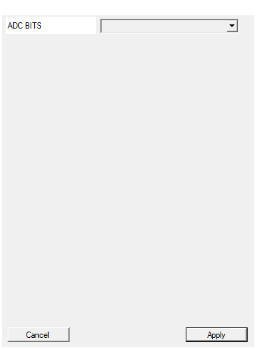
Set the number of raal bits of the board ADC
Default: 14
Options: 12 13 14 15 16
Usage
Architecture Overview
The IP integrates two identical signal processing chains for Side A and Side B:
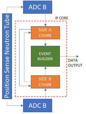
Each processing chain implements:
- Input stage - Offset subtraction and polarity inversion
- Signal filter - Quasi-Gaussian shaper (4th order)
- Trigger circuit - Threshold-based with hysteresis
- Peak detector - Maximum finder within gate window
- Output formatter - Packet generation with timestamp
Signal Processing Chain
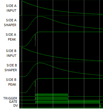
The filter chain consists of 5 cascaded blocks:
| Block | Function | Enable Bit |
|---|---|---|
| 1. Input Baseline | Removes DC offset from input | Bit 8 |
| 2. Pole-Zero | Compensates preamplifier decay | Bit 9 |
| 3. Gaussian Filter 1 | First 2nd-order section | Bit 10 |
| 4. Gaussian Filter 2 | Second 2nd-order section | Bit 11 |
| 5. Output Baseline | Removes DC offset from output | Bit 12 |
Each block can be enabled/disabled independently via the FLT_CFG register.
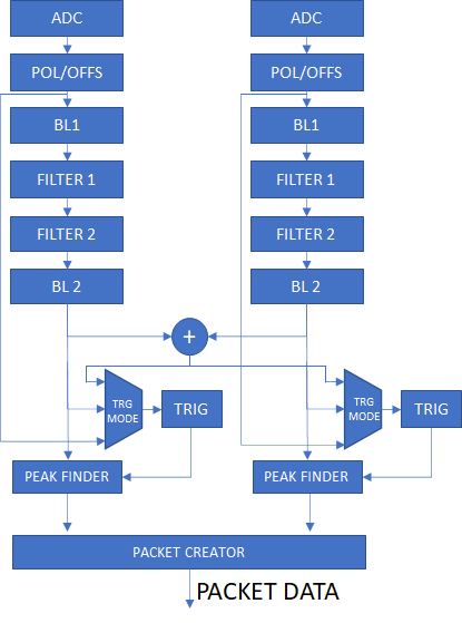
Input Stage
The input stage performs offset subtraction and optional polarity inversion:
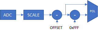
- OFFSET: DC offset value subtracted from the input signal
- POL: When POL=1, the signal is inverted (for negative pulses)
The Gaussian Shaper Filter Explained
The goal is to implement a quasi-Gaussian pulse shaper that transforms the detector signal into a shape suitable for amplitude measurement.
Why Gaussian Shaping?
A true Gaussian pulse shape is optimal for:
- Signal-to-noise ratio: Minimizes noise contribution
- Pile-up rejection: Clear separation between pulses
- Amplitude measurement: Peak corresponds to energy
The 4th-Order Approximation
The analog Gaussian filter uses this normalized transfer function:
$$ H(s) = \frac{4.899}{4.899 + 11.42s + 10.87s^2 + 5.073s^3 + s^4} $$
This filter has 4 complex poles in the s-plane:
- $s_{1,2} = -1.35536 \pm j \cdot 0.32795$
- $s_{3,4} = -1.18108 \pm j \cdot 1.0604$
Digital Implementation
Using the matched Z-transform method, we map the s-plane poles to z-plane poles:
$$ s_i \rightarrow e^{s_i \cdot T} $$
where $T = \frac{T_s}{2\pi\tau}$, $T_s$ is the sample period, and $\tau$ is the desired shaping time constant.
This results in two cascaded 2nd-order IIR filters (biquad sections):
$$ H_z(z) = \frac{K}{(1 - a_1 z^{-1} + b_1 z^{-2})(1 - a_2 z^{-1} + b_2 z^{-2})} $$
Each 2nd-order section is implemented as:
$$ u[n] = i[n] + a_k \cdot u[n-1] - b_k \cdot u[n-2] $$
Coefficient Calculation
The filter coefficients depend on two parameters:
- $\tau$ (tau): The Gaussian shaping time constant
- $f_{clk}$: The ADC/system clock frequency
First, calculate the normalized time:
$$ T = \frac{T_s}{2\pi\tau} = \frac{1}{2\pi \cdot \tau \cdot f_{clk}} $$
Then, the four coefficients are:
| Coefficient | Formula |
|---|---|
| $a_1$ | $2 \cdot e^{-1.35536 \cdot T} \cdot \cos(0.32795 \cdot T)$ |
| $b_1$ | $e^{-2.71072 \cdot T}$ |
| $a_2$ | $2 \cdot e^{-1.18108 \cdot T} \cdot \cos(1.0604 \cdot T)$ |
| $b_2$ | $e^{-2.36216 \cdot T}$ |
Understanding the formulas:
- The $a$ coefficients use $2 \cdot e^{-\text{real}} \cdot \cos(\text{imag})$ because they come from conjugate pole pairs
- The $b$ coefficients are simply $e^{-2 \cdot \text{real}}$ (the product of the two conjugate pole magnitudes)
Fixed-Point Scaling
For FPGA implementation, coefficients are scaled by 16384 ($2^{14}$):
| Register | Formula |
|---|---|
| COEFF11 | $\text{round}(b_1 \times 16384)$ |
| COEFF12 | $\text{round}(a_1 \times 16384)$ |
| COEFF21 | $\text{round}(b_2 \times 16384)$ |
| COEFF22 | $\text{round}(a_2 \times 16384)$ |
Pole-Zero Compensation
The pole-zero compensation circuit removes the exponential tail from the preamplifier output.
The Problem
A charge-sensitive preamplifier produces a signal with exponential decay:
$$ v(t) = V_0 \cdot e^{-t/\tau_l} $$
where $\tau_l$ is the long preamplifier time constant (typically 50-500 $\mu s$).
The Solution
We want to convert this to a shorter time constant $\tau_s$ (e.g., 8 sample periods). The transfer function is:
$$ H(s) = \frac{s + 1/\tau_l}{s + 1/\tau_s} $$
In digital form:
$$ w[n] = i[n] + \left(1 - \frac{T_s}{\tau_s}\right) \cdot w[n-1] $$
$$ u[n] = i[n] + \left(\frac{T_s}{\tau_l} - \frac{T_s}{\tau_s}\right) \cdot w[n] $$
PZCOEFF Calculation
The PZCOEFF register is scaled by 32768 ($2^{15}$):
$$ \text{PZCOEFF} = \text{round}\left(\frac{32768}{f_{clk} \cdot \tau_{pz}}\right) $$
where $\tau_{pz}$ is the preamplifier decay time constant.
Python Code for Coefficient Calculation
python
import math
def calculate_psa_coefficients(clock_freq_hz, tau_shaper_s, tau_pz_s):
"""
Calculate NI_PSA filter coefficients.
Parameters:
-----------
clock_freq_hz : float
ADC/system clock frequency in Hz (e.g., 125e6 for 125 MHz)
tau_shaper_s : float
Gaussian shaper time constant in seconds (e.g., 1e-6 for 1 us)
tau_pz_s : float
Preamplifier pole-zero time constant in seconds (e.g., 1e-6 for 1 us)
Returns:
--------
dict : Dictionary with coefficient names and integer values
"""
# Normalized time parameter
# T = Ts / (2 * pi * tau) = 1 / (2 * pi * tau * f_clk)
T = 1.0 / (2 * math.pi * tau_shaper_s * clock_freq_hz)
# Also written as: TS = (2 * pi) / (tau * clock_freq)
TS = (2 * math.pi) / (tau_shaper_s * clock_freq_hz)
# Gaussian filter poles (from 4th-order quasi-Gaussian approximation)
# Pole pair 1: -1.35536 +/- j*0.32795
# Pole pair 2: -1.18108 +/- j*1.0604
# First biquad section coefficients
# b1 = exp(-2 * real_part * T) = exp(-2.71072 * T)
# a1 = 2 * exp(-real_part * T) * cos(imag_part * T)
b1 = math.exp(-2.71072 * TS)
a1 = 2 * math.exp(-1.35536 * TS) * math.cos(0.327948 * TS)
# Second biquad section coefficients
b2 = math.exp(-2.36216 * TS)
a2 = 2 * math.exp(-1.18108 * TS) * math.cos(1.06037 * TS)
# Scale to fixed-point (14-bit precision, multiply by 16384)
coeff11 = int(b1 * 16384 + 0.5) # b1 scaled
coeff12 = int(a1 * 16384 + 0.5) # a1 scaled
coeff21 = int(b2 * 16384 + 0.5) # b2 scaled
coeff22 = int(a2 * 16384 + 0.5) # a2 scaled
# Pole-zero coefficient (15-bit precision, multiply by 32768)
pzcoeff = int(32768 / (clock_freq_hz * tau_pz_s))
return {
'COEFF11': coeff11,
'COEFF12': coeff12,
'COEFF21': coeff21,
'COEFF22': coeff22,
'PZCOEFF': pzcoeff,
'COEFF11_hex': f'0x{coeff11:04X}',
'COEFF12_hex': f'0x{coeff12:04X}',
'COEFF21_hex': f'0x{coeff21:04X}',
'COEFF22_hex': f'0x{coeff22:04X}',
'PZCOEFF_hex': f'0x{pzcoeff:04X}'
}
# Example usage
if __name__ == '__main__':
# Example: 125 MHz clock, 1 us shaping time, 1 us pole-zero
coeffs = calculate_psa_coefficients(
clock_freq_hz=125e6,
tau_shaper_s=1e-6,
tau_pz_s=1e-6
)
print("NI_PSA Filter Coefficients")
print("=" * 40)
print(f"COEFF11 (b1): {coeffs['COEFF11']:5d} = {coeffs['COEFF11_hex']}")
print(f"COEFF12 (a1): {coeffs['COEFF12']:5d} = {coeffs['COEFF12_hex']}")
print(f"COEFF21 (b2): {coeffs['COEFF21']:5d} = {coeffs['COEFF21_hex']}")
print(f"COEFF22 (a2): {coeffs['COEFF22']:5d} = {coeffs['COEFF22_hex']}")
print(f"PZCOEFF : {coeffs['PZCOEFF']:5d} = {coeffs['PZCOEFF_hex']}")
# Verify with known values from documentation
# For tau=1us, pz=1us, 125MHz: coeff11=0x37d9, coeff12=0x778e, etc.
Example Coefficient Values
| Clock | Shaping Time | COEFF11 | COEFF12 | COEFF21 | COEFF22 | PZCOEFF |
|---|---|---|---|---|---|---|
| 125 MHz | 1.0 $\mu s$ | 0x37D9 | 0x778E | 0x38D6 | 0x7873 | 0x0106 |
| 125 MHz | 2.0 $\mu s$ | 0x3BDB | 0x7B97 | 0x3C60 | 0x7C1C | 0x0106 |
| 80 MHz | 1.0 $\mu s$ | 0x3543 | 0x74EA | 0x3656 | 0x75E5 | 0x019A |
Baseline Correction Algorithm
The baseline correction removes DC offset and compensates for AC coupling effects:
- Divide samples into chunks of N samples
- Find the minimum value in each chunk
- Apply first-order IIR filter to smooth the minimum: $$ w[n] = \frac{1}{k} \cdot \min[n] + \left(1 - \frac{1}{k}\right) \cdot w[n-1] $$
- Subtract the smoothed baseline from input: $u[n] = i[n] - w[n]$
Default: $k = 32$ (implemented as bit shift)
Trigger System
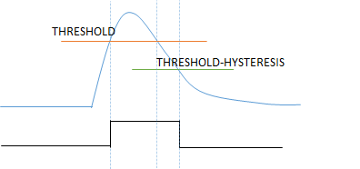
Trigger modes (TRG_MODE):
- 0: Sum of both sides (A + B)
- 1: External trigger only
- 2: OR of both sides (A OR B)
- 3: AND of both sides (A AND B)
Trigger features:
- Programmable threshold (TRG_THRES)
- Hysteresis to prevent noise re-triggering (TRG_HIST)
- Holdoff time after trigger (TRG_HOLD)
- Configurable output width (TRG_OUT_W)
Maximum Finder (Peak Detection)
When triggered, the peak detector:
- Opens a gate window (GATE_W clock cycles)
- Monitors the sum signal (A + B)
- Stores the maximum sum value and corresponding A/B values
- At gate close, outputs the stored peak values
Pile-up handling:
- If a new trigger occurs during the gate window, the event is marked as pile-up
- The second event is discarded
Output Data Format
The DATA output is a 128-bit packet:

| Bits | Field | Description |
|---|---|---|
| 127:64 | TIMESTAMP | 64-bit timestamp value |
| 63:48 | CH_ID | 12-bit channel ID + 4-bit flags |
| 47:32 | SIDE_A | 16-bit energy from Side A |
| 31:16 | SIDE_B | 16-bit energy from Side B |
| 15:0 | SUM | 16-bit energy sum (A + B) |
Flag bits in CH_ID field:
- Bit 0: PILEUP_A
- Bit 1: PILEUP_B
- Bit 2: OVR_A (overflow)
- Bit 3: OVR_B (overflow)
Resources & Timing
-
Latency: Variable (depends on filter configuration)
-
Throughput: 1 event per gate window duration
Uses DSP blocks for filter multiplications. Filter configuration and coefficients must be properly calculated for optimal performance.