SCI-Compiler Development Kit - DT1260 (SciDK)
The SCI-Compiler Development Kit (SciDK) based on the DT1260 board is an entry-level platform designed for learning FPGA programming through block-diagram-based design. This guide covers the hardware specifications, features, and capabilities of the DT1260 dual-channel digitizer with open FPGA architecture.
Introduction
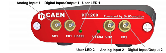
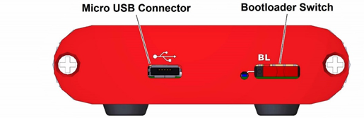
The SCI-Compiler SMART Kit is designed for non-expert users approaching FPGA programming for the first time. It introduces an innovative method to simplify firmware development based on SCI-Compiler software — a block-diagram-based programming interface with a prebuilt set of functions specifically developed for physics and engineering applications.
By placing and interconnecting available blocks (oscilloscope, TDC, MCA, charge integration, etc.) on a diagram, SCI-Compiler automatically generates VHDL code that implements the required function and deploys it to the FPGA. Even non-expert users can write custom firmware without any knowledge of VHDL/Verilog programming languages.
SCI-Compiler SMART Kit Contents
The kit includes everything needed to start learning FPGA programming:
| Component | Description |
|---|---|
| 1× DT1260 | 2-channel, 65 MS/s, 12-bit ADC unit with Open FPGA (also called SciDK board) |
| 1× SCI-Compiler Lite License | Software license working with DT1260 unit only |
| USB Cable | For programming and data communication |
| Quick Start Guide | Getting started documentation |
What You Can Do with the Kit
The SCI-Compiler software, in combination with DT1260, enables you to develop:
- FPGA Firmware for custom digital pulse processing
- Software Applications for data readout using auto-generated libraries
- Register Access to control DT1260 parameters
- Data Transfer to PC in list, waveform, or custom formats
Learning Path
The kit is designed for progressive learning:
1. Example Firmware Projects
SCI-Compiler includes multiple example firmware diagrams to help you:
- Understand block-diagram programming concepts
- Learn FPGA design patterns
- Build confidence with the software
- Experiment with real hardware immediately
2. Hands-On Labs
Complete the SCI-Compiler Hands-On Labs available at:
These labs guide you through:
- Basic digital logic
- Signal processing algorithms
- Data acquisition systems
- Custom firmware development
3. Community Support
Join the community forum for help and discussions:
DT1260 Hardware Specifications
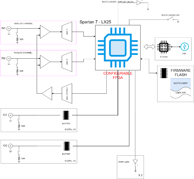
The DT1260 is a dual-channel, open FPGA Flash ADC unit. The core of the system is a programmable Xilinx Spartan-7 XC7S25 FPGA, fully compatible with SCI-Compiler software.
Technical Specifications
| Specification | Value |
|---|---|
| Analog Channels | 2 (single-ended, LEMO connectors) |
| ADC Resolution | 12 bits |
| Sampling Rate | 65 MS/s per channel |
| Input Range | 2 Vpp (±1V around offset) |
| Bandwidth | 30 MHz |
| Input Coupling | DC |
| Input Impedance | 1 kΩ / 50 Ω (jumper selectable) |
| DC Offset | Programmable via 12-bit DAC |
| Digital I/O | 2 programmable TTL (LEMO) |
| User LEDs | 2 programmable |
| FPGA | Xilinx Spartan-7 XC7S25-1FTGB196C |
| Logic Cells | 23,360 |
| Block RAM | 1.8 Mb (225 KB) |
| DSP Slices | 80 |
| Flash Memory | 128 Mbit (user firmware storage) |
| Interface | USB 2.0 High Speed (480 Mbps) |
| Power Supply | USB bus-powered |
| Power Consumption | < 2 W |
| Dimensions | Compact desktop form factor |
FPGA Resources
The Spartan-7 XC7S25 provides sufficient resources for complex algorithms:
What You Can Implement
| Application | Feasibility |
|---|---|
| Trapezoidal filter | ✓ Yes — full energy reconstruction |
| Digital shapers | ✓ Yes — CR-RC, CR-RC², Gaussian |
| Baseline restoration | ✓ Yes — moving average, exponential |
| Trigger logic | ✓ Yes — threshold, CFD, leading edge |
| Oscilloscope | ✓ Yes — up to 500 µs buffer per channel |
| Spectrum (MCA) | ✓ Yes — 1K to 16K bins |
| List mode | ✓ Yes — time-tagged events |
| Custom algorithms | ✓ Yes — within resource limits |
Buffer Memory Limitations
No external RAM is available on the DT1260. All buffers must fit in the 225 KB of on-chip Block RAM.
Example waveform buffer capacity:
- Single channel: Up to 90K samples (~1.4 ms at 65 MS/s)
- Dual channel: Up to 45K samples per channel (~700 µs)
For most applications (pulse processing, spectroscopy, TDC), this memory is sufficient. For long waveform recording, use a larger board like DT5560.
Analog Front-End
Input Configuration
The analog input is connected to a buffer with offset regulation on the inverting input:
LEMO IN ──► [Termination] ──► [Buffer + Offset] ──► ADC
↓
1kΩ or 50Ω
Default impedance: 1 kΩ (high impedance)
50 Ω termination: Available by opening the enclosure and installing jumpers on the PCB.
DC Offset Control
The analog input offset is regulated via an integrated 12-bit DAC. SCI-Compiler exports a default ANALOG_OFFSET register.
How it works:
- Write a 12-bit value (0-4095) to the ANALOG_OFFSET register
- The DAC adjusts the DC offset to move the ADC baseline to that level
Example:
python
# Set baseline at mid-scale (2048)
sdk.SetParameter("board0:/Registers/ANALOG_OFFSET", 2048)
Result: 0V input signal appears at ~2048 ADC counts.
Input Dynamic Range
The input dynamic is 2 Vpp:
| Input Voltage | ADC Code | Usage |
|---|---|---|
| -1V | 0 | Minimum |
| 0V | ~2048 | Mid-scale (with offset = 2048) |
| +1V | 4095 | Maximum |
Signal polarity recommendations:
| Signal Type | Recommended Offset | Dynamic Coverage |
|---|---|---|
| Positive only | 0 | 0V to +2V → 0 to 4095 |
| Negative only | 4095 | 0V to -2V → 4095 to 0 |
| Bipolar | 2048 | -1V to +1V → 0 to 4095 (symmetric) |
Digital I/O
Programmable I/O Channels
- 2× TTL I/O on LEMO connectors
- Direction configurable in firmware (input or output)
- 3.3V LVTTL logic levels
Configuration in SCI-Compiler:
Use the Digital I/O block in your diagram:
- Drag the block onto the design
- Select the pin (DIO0, DIO1)
- Configure as Input or Output
- Connect to your processing logic
Example use cases:
- Output: Trigger out, gate signals, event markers
- Input: External trigger, veto, gate input
USB Communication
Interface Specifications
- Standard: USB 2.0 High Speed
- Throughput: Up to 40 MB/s sustained
- Latency: < 1 ms
- Power: Bus-powered (no external supply needed)
Data Transfer Modes
SCI-Compiler supports multiple data acquisition modes:
| Mode | Description | Throughput |
|---|---|---|
| Registers | Read/write configuration | Very low |
| Oscilloscope | Triggered waveform capture | 1-10 MB/s |
| Spectrum | Histogram accumulation | Very low |
| List | Event-by-event streaming | Up to 40 MB/s |
| Custom Packet | User-defined data structures | Up to 40 MB/s |
Firmware Storage
Flash Memory Organization
The DT1260 includes 128 Mbit (16 MB) Flash memory:
| Region | Size | Content | User Access |
|---|---|---|---|
| Bootloader | ~4 MB | Factory-programmed USB bootloader | Read-only |
| User Firmware | ~12 MB | SCI-Compiler generated bitstream | Read/write |
Fast Bootloader
The factory-programmed bootloader enables:
- Fast programming via USB (no JTAG needed)
- Automatic enumeration when connected to PC
- Firmware upgrade directly from SCI-Compiler
- Persistent storage — firmware retained after power-off
Programming time: Typically 10-30 seconds
User LEDs
LED Control
- 2× User LEDs on the front panel
- Programmable from firmware
- Indicators for custom status, debugging, or events
Example use in SCI-Compiler:
Add a LED Driver block:
- Connect to trigger signal → LED blinks on events
- Connect to counter overflow → LED indicates buffer full
- Connect to error flag → LED shows fault condition
Connector Pinout
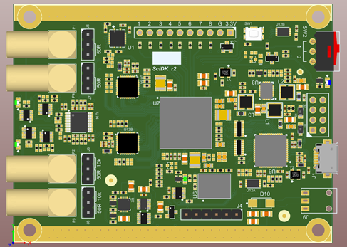
Front Panel Connectors
| Connector | Type | Function |
|---|---|---|
| IN 0 | LEMO | Analog input channel 0 |
| IN 1 | LEMO | Analog input channel 1 |
| DIO 0 | LEMO | Digital I/O 0 (programmable) |
| DIO 1 | LEMO | Digital I/O 1 (programmable) |
| USB | Micro-USB | Communication + Power |
Internal Headers (Require Opening Enclosure)
| Header | Function |
|---|---|
| JTAG | Direct FPGA programming (for advanced users) |
| Termination jumpers | Select 50Ω or 1kΩ input impedance |
Typical Applications
The DT1260 is ideal for learning and prototyping:
Educational Applications
- University labs — Teach FPGA design without HDL complexity
- Student projects — Implement custom instruments
- Research prototyping — Test algorithms before deploying to larger systems
Signal Processing Examples
| Project | Description |
|---|---|
| Pulse Height Analysis (PHA) | Energy spectroscopy with trapezoidal filter |
| Time-of-Flight (ToF) | Timing measurements with TDC |
| Waveform Digitizer | Triggered oscilloscope with pretrigger |
| Coincidence Logic | Multi-channel trigger systems |
| Custom Trigger | CFD, leading edge, threshold discrimination |
| Baseline Restoration | Moving average, exponential decay |
Physics & Engineering
- Radiation detector readout (PMT, SiPM, semiconductor)
- Scintillator spectroscopy (NaI, CsI, LaBr3)
- Timing experiments (coincidence, ToF)
- Custom pulse processing (shaping, filtering)
Comparison with Other Platforms
| Feature | DT1260 (SciDK) | DT5560 | R5560 |
|---|---|---|---|
| Purpose | Learning, evaluation | Laboratory R&D | Production systems |
| Channels | 2 | 8-16 | 128 |
| Sampling Rate | 65 MS/s | 125 MS/s | 125 MS/s |
| Resolution | 12-bit | 14-bit | 14-bit |
| FPGA | Spartan-7 XC7S25 | Zynq-7030 | 4× Zynq-7030 |
| Logic Cells | 23K | 125K | 500K |
| External RAM | None | 1 GB DDR3 | 4 GB DDR3 |
| Form Factor | Compact desktop | Desktop | 2U rackmount |
| Price | Entry-level | Mid-range | High-end |
DT1260 Advantages:
- Lowest cost for learning
- USB-powered (no external supply)
- Compact, portable
- Sufficient for most learning projects
When to Upgrade:
- Need more channels (DT5560, R5560)
- Require higher resolution (DT5560, R5560)
- Need large waveform buffers (DT5560, R5560)
- Production deployment (R5560)
Getting Started Guide
Step 1: Unboxing
- Remove DT1260 from packaging
- Connect USB cable (micro-USB on device, USB-A on PC)
- Power LED should illuminate
Step 2: Install SCI-Compiler
- Download SCI-Compiler from sci-compiler.com
- Install software
- Activate your SCI-Compiler Lite license (included with kit)
Step 3: Connect Hardware
- Launch SCI-Compiler
- Go to Tools → Hardware Manager
- Click Detect Devices
- DT1260 should appear in the device list
Step 4: Load Example Project
- Go to File → Open Example
- Select DT1260 → Simple Oscilloscope
- Click Compile
- Wait for compilation (~10 minutes first time)
- Firmware is automatically downloaded to DT1260
Step 5: Test with Resource Explorer
- Go to Tools → Resource Explorer
- Connect to DT1260
- Navigate to Oscilloscope_0
- Connect a signal to IN 0 (or leave floating to see noise)
- Click Arm and Start
- View waveform in real-time
Step 6: Modify and Experiment
- Open the block diagram
- Change parameters (threshold, trigger mode, etc.)
- Add processing blocks (filters, baseline)
- Recompile and test
- Iterate and learn!
Advanced Features
Using the 50Ω Termination
For high-frequency signals or impedance-matched systems:
- Power off the DT1260
- Open the enclosure (remove screws on bottom)
- Locate termination jumpers near analog inputs
- Install jumpers to enable 50Ω termination
- Close enclosure and power on
Warning: Always power off before opening the enclosure.
JTAG Programming (Advanced)
For advanced users who want direct FPGA access:
- JTAG header available on PCB
- Compatible with Xilinx Platform Cable USB II
- Use Vivado for low-level debugging and development
Note: For normal operation, use SCI-Compiler’s USB bootloader.
Troubleshooting
Device Not Detected
Problem: DT1260 not appearing in Hardware Manager
Solutions:
- Check USB cable connection
- Try different USB port (avoid hubs)
- Install/update USB drivers (automatic with SCI-Compiler)
- Restart SCI-Compiler
- Check power LED is on
Compilation Errors
Problem: Firmware compilation fails
Solutions:
- Check all blocks are connected
- Verify parameters are within valid ranges
- Review error messages in console
- Try a simpler design first
- Ensure Xilinx Vivado is installed and licensed
No Signal on Oscilloscope
Problem: Waveform shows flat line
Solutions:
- Check analog input cable
- Verify signal amplitude is within ±1V
- Adjust DC offset (ANALOG_OFFSET register)
- Check trigger settings (try Auto trigger mode)
- Verify firmware is running (check status LED)
Offset Adjustment Not Working
Problem: Setting ANALOG_OFFSET has no effect
Solutions:
- Check register address in firmware
- Verify DAC is enabled in design
- Use values 0-4095 (12-bit range)
- Allow 100ms for DAC to settle
Resources and Support
Documentation
- SCI-Compiler User Manual: Included with software installation
- Hands-On Labs: https://www.sci-compiler.com/hands-on/
- Block Reference Guide: Available in SCI-Compiler Help menu
Community
- Forum: https://community.sci-compiler.com
- Support email: support@sci-compiler.com
Upgrades
When you’re ready for more advanced projects:
- SCI-Compiler Professional License — Unlock all supported boards
- DT5560 Desktop Digitizer — 8-16 channels, 125 MS/s, 14-bit, Zynq FPGA
- R5560 Rackmount System — Up to 128 channels for production systems
Summary
The DT1260 SCI-Compiler Development Kit provides everything you need to:
- ✓ Learn FPGA programming without HDL expertise
- ✓ Design custom signal processing algorithms visually
- ✓ Test ideas with real hardware immediately
- ✓ Build confidence before tackling larger systems
- ✓ Access a complete block library for common tasks
- ✓ Generate working firmware and software automatically
Perfect for:
- Students learning digital signal processing
- Researchers prototyping custom instruments
- Engineers evaluating FPGA-based solutions
- Anyone curious about programmable hardware
Start your FPGA journey today with the SciDK!