Getting Started with V2495 (Pattern Generator & Logic Analyzer)
Step-by-step tutorial for CAEN V2495 VME board. Learn to create a complete firmware design using Pattern Generator, Logic Analyzer, counters, and registers. Test with Resource Explorer including table views, plots, and graphical signal display. Complete guide for digital signal generation and analysis applications.
Introduction
This tutorial demonstrates how to design firmware for the CAEN V2495 VME board to generate and analyze digital signals. The example implements a complete system with random pattern generation, logic analysis, and event counting.
About the V2495
The CAEN V2495 is a general-purpose VME board with an open FPGA, designed for custom logic and signal processing applications:
- Xilinx Spartan-6 FPGA (XC6SLX150T)
- 32 differential I/O channels (LVDS/NIM/TTL compatible)
- VME64 and USB connectivity
- 96-pin expansion connector for custom piggybacks
- High-speed serial links (optical and electrical)
- On-board memory (SRAM and Flash)
What You’ll Learn
- Creating a new V2495 project in SCI-Compiler
- Using the Pattern Generator block
- Implementing Logic Analyzer for signal visualization
- Adding Rising Edge Counters
- Working with Registers (read/write)
- Memory mapping and address assignment
- Compiling and programming the FPGA
- Testing with Resource Explorer (tables, plots, logic analyzer)
Project Overview
This example firmware implements:
- Pattern Generator - Generates 16-bit random digital patterns
- Wire Split - Splits 16-bit pattern into 16 individual signals
- Logic Analyzer - Captures and visualizes all 16 signals
- 16 Rising Edge Counters - Count transitions on each channel
- 17 Registers - Store counter values (16) plus reset register (1)
Step 1: Create the Project
Launch SCI-Compiler
- Run SCI-Compiler
- In the starting window, click the V2495 button
- Enter a Project Name
- Enter or browse to a Project Folder
- Click Create
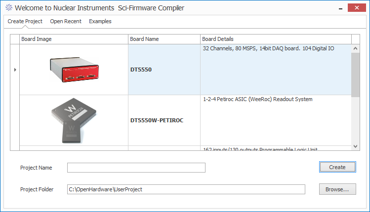
Figure 1: Creating a new V2495 project
The project will be created with the basic board infrastructure pre-configured.
Step 2: Create the Registers
Registers allow reading counter values and controlling the firmware.
Add Counter Registers (16 registers)
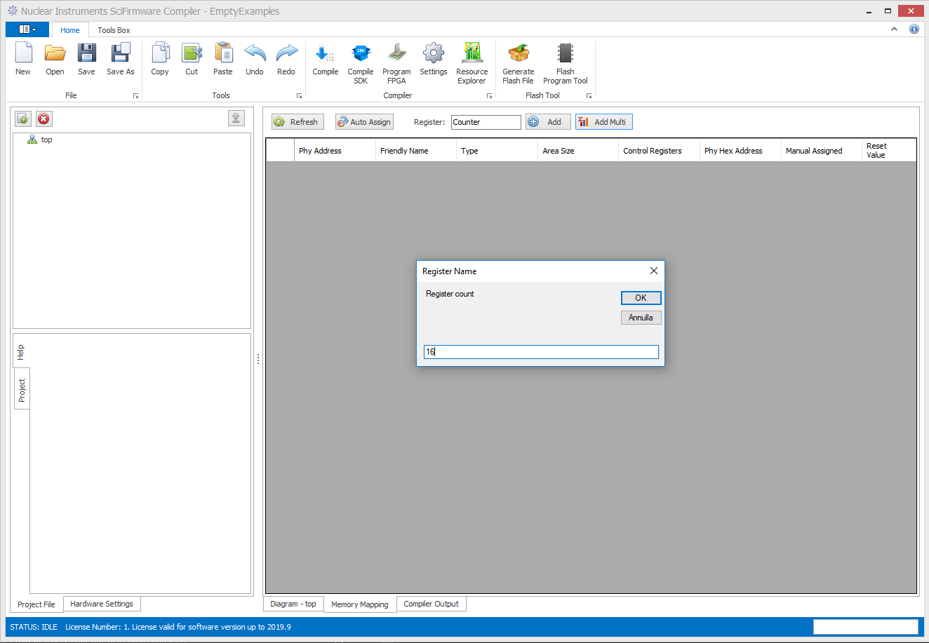
Figure 2: Adding multiple registers
- Click the Memory Mapping tab at the bottom
- Enter a name in the Register field (e.g., “CNT”)
- Click Add Multi button
- In the popup window, enter 16 as the number of registers
- Click OK
The registers will be automatically created with incremental names (CNT_0, CNT_1, … CNT_15).
Add Reset Register
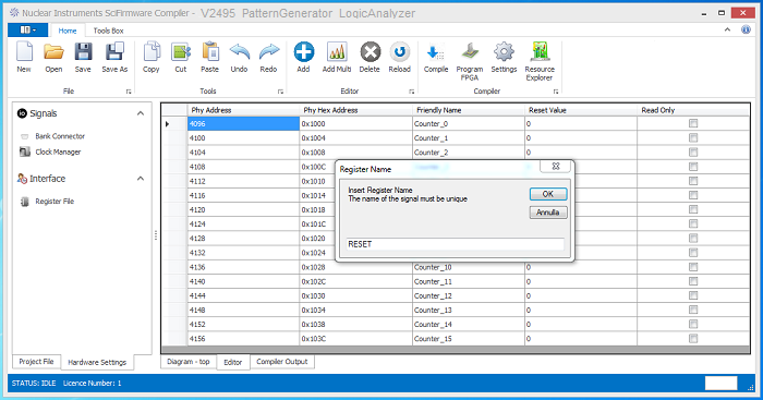
Figure 3: Adding the reset register
- Enter “RESET” in the Register field
- Click Add button
You should now have 17 registers total in the Editor tab.
Step 3: Add the Pattern Generator
The Pattern Generator creates random digital patterns from a file.
Create Random Number File
First, create a text file containing random hexadecimal numbers (0 to FFFF), one per line:
A3F5
12BC
FF00
...
Configure Pattern Generator Block
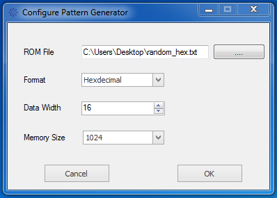
Figure 4: Pattern Generator configuration
- In the Tools Box toolbar, click Delay Memory button (in Logic group)
- Select Pattern Generator from the sub-menu
- In the configuration window:
- ROM File: Browse to your random numbers file
- Format: Hexadecimal
- Data Width: 16
- Memory Size: 1024
- Click OK
Add Clock Divider
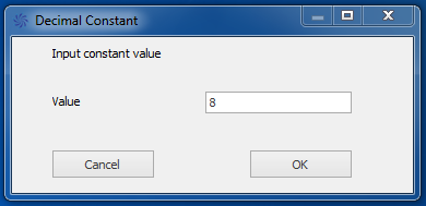
Figure 5: Adding a constant for clock division
To slow down pattern generation:
- Click Misc button in Wire group
- Select Constant (INT)
- Set Value: 8
- Click OK
- Connect the constant to the CLK DIV input of the Pattern Generator
Step 4: Add Wire Split
Split the 16-bit pattern into 16 individual 1-bit signals.
Configure Wire Split Block
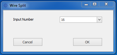
Figure 6: Wire Split configuration
- Click Wire Split in the Binary Operations sub-menu (Wire group)
- Select 16 as the number of output bits
- Click OK
- Connect the OUT pin of Pattern Generator to the IN pin of Wire Split
Step 5: Add Logic Analyzer
The Logic Analyzer captures and displays digital signals.
Configure Logic Analyzer Block
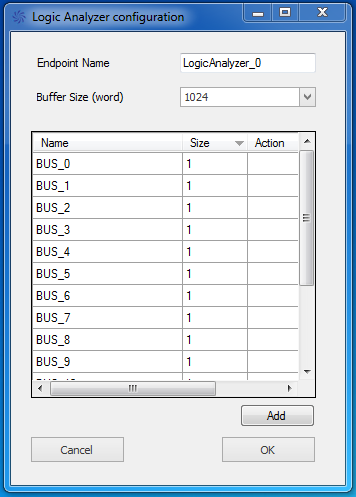
Figure 7: Logic Analyzer configuration
- Click DAQ button (Signal Processing group)
- Select Logic Analyzer
- In the configuration window:
- Buffer Size (word): 1024
- Click Add button 16 times to create 16 channels
- Each channel should have size 1
- Click OK
Connect Signals to Logic Analyzer
- Connect each output pin of Wire Split to an input pin of Logic Analyzer
- Tip: Use keyboard shortcut Alt+R to auto-replicate connections:
- Create the first link
- Select it
- Press Alt+R
- Enter 15 (to create 15 more links)
Add Trigger Signal
- Click Misc → True to create a constant True block
- Connect the True block to the TRIGGER input of Logic Analyzer
Step 6: Add Counters
Add 16 Rising Edge Counters to count signal transitions.
Create Counter Blocks
- Click Timer Counters sub-menu (Logic group)
- Select Rising Edge Counter
- Add one counter, then copy/paste 15 times for total of 16
Connect Counters
- Connect each Wire Split output to an in input of a Counter block
- Tip: Use keyboard shortcut Alt+F:
- Create first link
- Press Alt+F
- Click on all destination Counter blocks
Add Gate Signal
- Create another True constant
- Connect it to the GATE input of each Counter
- Tip: Use Alt+E to auto-connect:
- Create first link
- Select it
- Press Alt+E
- Click on all Counter blocks
Step 7: Add Counter Output Registers
Connect counters to registers for readout.
Create Register Write Blocks
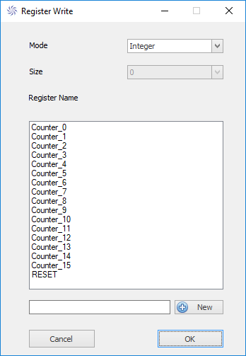
Figure 8: Register write blocks connected to counters
- Click Register button (Communication group)
- Select Register Write
- In the configuration window:
- Select all 16 counter registers (CNT_0 through CNT_15)
- Mode: Bit Vector
- Size: 32
- Click OK
Connect Counter Outputs
- Connect Counts output of each Counter to corresponding Register block
- Tip: Use Alt+S shortcut:
- Select first link
- Press Alt+S
- Click on each Counter block in sequence
Enable Register Writing
- Create a True constant
- Connect to WR input of each Register block
- Use Alt+E to auto-connect
Add Reset Functionality
- Click Register → Register Read
- Select the RESET register
- Set as Bit Vector, size 1
- Click OK
- Connect the RESET Register to each Reset input of Counter blocks
- Use Alt+E to auto-connect
Step 8: Complete Diagram
Your final block diagram should look like this:
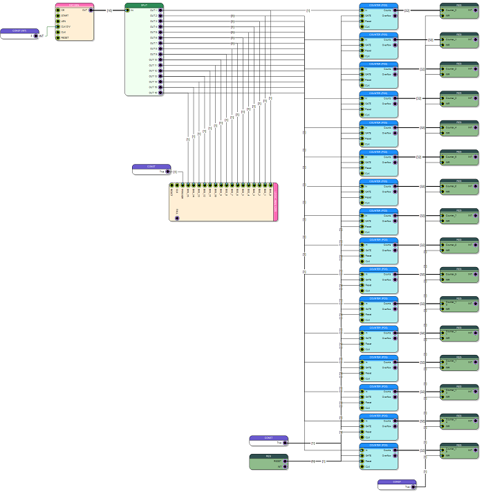
Figure 9: Complete firmware block diagram
Verify all connections:
- Pattern Generator → Wire Split → Logic Analyzer
- Pattern Generator → Wire Split → Counters → Registers
- True constants → Logic Analyzer TRIGGER
- True constants → Counter GATE inputs
- True constants → Register WR inputs
- RESET register → Counter Reset inputs
Step 9: Compile the Project
Start Compilation
- Select the Home toolbar
- Click Compile button
- SCI-Compiler launches Quartus and shows output in Compiler Output tab
- Wait 10-20 minutes for compilation
- Upon success, you’ll see “Successful Compilation!”
Generated files:
.rpdfile (FPGA bitstream).jsonfile (RegisterFile.json in library folder)
Step 10: Program the FPGA
Hardware Connections
Ensure the V2495 board is:
- Powered on
- Connected via USB cable or VME/optical link
- Recognized by your computer
Download Firmware
- Click Program FPGA button in Home toolbar
- SCI-Compiler automatically:
- Detects programming cable
- Connects to FPGA
- Downloads firmware
- Wait for “Target device programmed successfully”
Testing with Resource Explorer
Launch and Connect
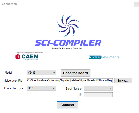
Figure 10: Connecting to the V2495 board
- Click Resource Explorer button
- In the Connection window:
- Select V2495 board
- Choose Connection Type (USB, Optical, or VME)
- Select correct Serial Number or IP
- Verify Select Json File path is correct (auto-filled)
- Click Connect
After connection, the available resources appear:
- Registers (CNT_0 through CNT_15, RESET)
- LogicAnalyzer_0
Using Table View for Registers
Create a Table
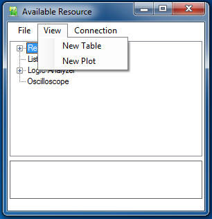
Figure 11: Creating a new table
- Click View menu
- Select New Table
- Table 0 will be created
Add Registers to Table
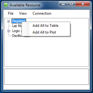
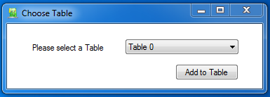
Figure 12: Adding registers to table
- Right-click on Registers
- Click Add All to Table
- Select Table 0 in Choose Table dialog
- Click Add to Table
Read Register Values
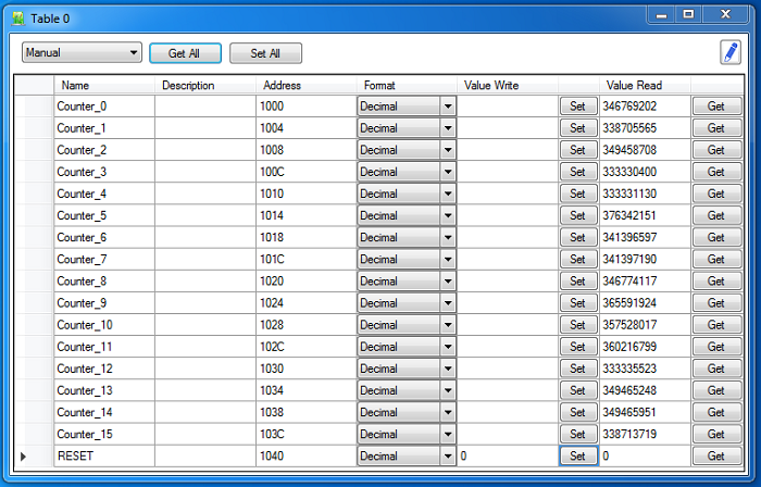
Figure 13: Table view with register values
Manual reading:
- Click Get All to read all registers once
Auto-update:
- Select refresh rate: Auto 50 ms, Auto 100 ms, Auto 500 ms, Auto 1 s, Auto 10 s
- Values update automatically
You’ll see counter values incrementing as signals are counted.
Using Plot View for Registers
Create a Plot
- Click View menu → New Plot
- Plot 0 will be created
Add Registers to Plot
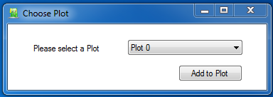
Figure 14: Adding registers to plot
- Right-click on Registers
- Click Add All to Plot
- Select Plot 0
- Click Add to Plot
Display Register Trends
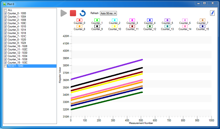
Figure 15: Plot view showing counter trends
Control the plot:
- Check/uncheck registers to show/hide traces
- Use ALL checkbox to toggle all at once
- Select Refresh rate
- Click
to start acquisition
- Click
to stop
- Click
to clear data
Using Logic Analyzer View
Open Logic Analyzer
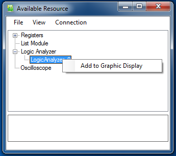
Figure 16: Opening Logic Analyzer graphic display
- Right-click on LogicAnalyzer_0
- Select Add to Graphic Display
Configure and Acquire
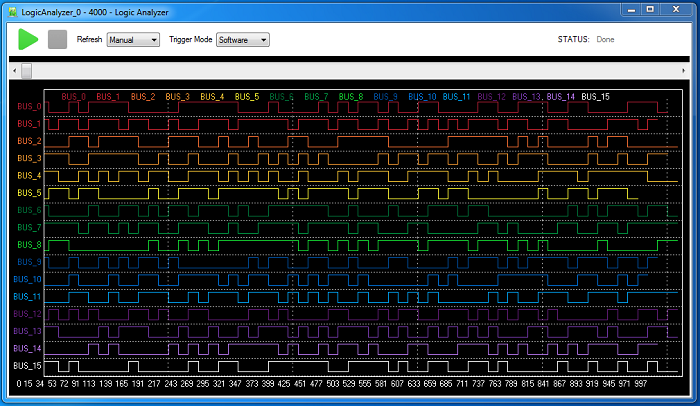
Figure 17: Logic Analyzer showing 16 digital signals
Settings:
- Refresh: Manual or Auto
- Trigger Mode:
- Software - Free running
- Signal - Use TRIGGER input (set to 1 in this example)
Controls:
- Click
to start acquisition
- Click
to stop acquisition
- Each of the 16 buffers displays in a different color
- Zoom and pan to inspect signal details
You’ll see the random digital patterns being generated on all 16 channels!
Understanding the Design
Data Flow
Random File → Pattern Generator → 16-bit Pattern
↓
Wire Split → 16 individual bits
↓
┌─────┴─────┐
↓ ↓
Logic Analyzer Counters → Registers → USB Readout
Pattern Generator Operation
- Reads values from ROM file (random hex numbers)
- Outputs 16-bit word on each clock cycle
- Clock divided by 8 (via CLK DIV input)
- Cycles through memory (1024 values)
Counter Operation
- Detects rising edges (0→1 transitions)
- Increments internal counter
- Value written to register continuously
- Can be reset via RESET register
Logic Analyzer Operation
- Samples all input channels simultaneously
- Stores 1024 samples per channel in buffer
- Triggers on software command or signal edge
- Transfers buffer to PC via USB
Advanced Topics
Using Real Inputs
Instead of Pattern Generator, connect external signals:
- Remove Pattern Generator and Wire Split
- Add Board Input blocks from Board menu
- Connect V2495 physical inputs to counters and logic analyzer
- Process real digital signals from detectors, sensors, etc.
Adding Digital Outputs
Output processed signals to V2495 outputs:
- Add Board Output blocks
- Connect your logic to output pins
- Generate triggers, gates, or control signals
- Drive external instrumentation
Trigger Logic
Implement custom trigger conditions:
- Use Boolean Logic blocks (AND, OR, NOT)
- Add Comparators for threshold detection
- Implement Coincidence logic
- Create Delayed triggers
- Use Pulse Generators for gate signals
Rate Meters
Convert counters to rate meters:
- Add Rate Meter block from Logic group
- Connect signal inputs
- Specify time base (e.g., 1 second)
- Read rate in Hz instead of total counts
List Mode Acquisition
Record event data to PC:
- Add List endpoint block
- Pack timestamp, channel, and data
- Stream events to PC via USB
- Analyze offline with SciSDK
Multi-Board Systems
Synchronize multiple V2495 boards:
- Use Clock Distribution outputs
- Implement Busy Logic for coordination
- Share Common Trigger
- Merge data streams in software
Keyboard Shortcuts Reference
SCI-Compiler provides shortcuts to speed up wiring:
| Shortcut | Function | Usage |
|---|---|---|
| Alt+R | Replicate link | Select link, press Alt+R, enter count |
| Alt+F | Fan-out from source | Create link, press Alt+F, click destinations |
| Alt+E | Fan-out to destinations | Create link, select it, press Alt+E, click destinations |
| Alt+S | Serial connection | Select link, press Alt+S, click blocks in sequence |
Troubleshooting
Compilation Fails
Problem: Quartus reports errors during compilation
Solutions:
- Check all blocks have valid parameters
- Verify all inputs are connected
- Ensure no unconnected required pins
- Check resource usage (FPGA may be too full)
- Review Compiler Output for specific errors
Cannot Program FPGA
Problem: “Target device programmed successfully” doesn’t appear
Solutions:
- Verify board is powered on
- Check USB cable connection
- Ensure drivers are installed
- Try different USB port
- Check if board is detected by Windows Device Manager
- For VME: verify VME crate and controller
Resource Explorer Cannot Connect
Problem: Connection fails or times out
Solutions:
- Verify firmware is programmed
- Check JSON file path is correct
- Ensure USB connection is stable
- Try different connection type (USB vs. VME/optical)
- Restart Resource Explorer
- Power cycle the board
Logic Analyzer Shows No Data
Problem: Empty or frozen display
Solutions:
- Verify trigger mode is correct
- Check TRIGGER input is connected
- Ensure Pattern Generator is running
- Try manual trigger (software mode)
- Check CLK DIV constant value
- Verify all signal connections
Counters Not Incrementing
Problem: Register values stay at zero
Solutions:
- Check GATE inputs are enabled (True constant)
- Verify signal connections from Wire Split
- Ensure Pattern Generator is outputting data
- Check WR inputs of registers are enabled
- Verify counter hasn’t overflowed
Counters Reset Unexpectedly
Problem: Values go back to zero
Solutions:
- Check RESET register value (should be 0)
- Don’t write 1 to RESET register
- Verify no spurious reset signals
- Check counter bit width (32-bit should be sufficient)
Typical Applications
Digital Signal Processing
- Trigger Logic for particle detectors
- Coincidence Systems for PET/SPECT
- Event Builders for multi-detector arrays
- Gate Generators for acquisition windows
- Dead-Time Logic for high rate experiments
DAQ Systems
- Multi-Channel Counting (scaler)
- Time-to-Digital Conversion (TDC)
- Pulse Pattern Recognition
- Serial Protocol Interfaces (SPI, I2C, UART)
- Custom Readout Controllers
Test and Measurement
- Pattern Generation for testing
- Signal Analysis and debugging
- Protocol Analyzers (digital communication)
- Pulse Generators with programmable patterns
- Timing Generators for synchronization
Control Systems
- Interlock Logic for safety systems
- State Machines for process control
- Sequence Generators for automation
- Feedback Controllers (digital)
- Alarm Logic with multiple conditions
Summary
This tutorial covered V2495 firmware design from start to finish:
| Topic | Covered |
|---|---|
| Project creation | New V2495 project setup |
| Register management | Creating, naming, memory mapping |
| Block diagram design | Pattern Generator, Wire Split, Logic Analyzer, Counters |
| Wiring techniques | Manual connections and keyboard shortcuts |
| Compilation | Quartus integration and bitstream generation |
| FPGA programming | Download firmware via USB/VME |
| Resource Explorer | Tables, plots, logic analyzer display |
| Testing | Real-time monitoring and data visualization |
Key Skills Acquired:
- Complete firmware design workflow
- Using SCI-Compiler blocks and tools
- Resource Explorer testing techniques
- Real-time data monitoring and plotting
- Digital signal analysis
Next Steps:
- Modify pattern source for different signals
- Add external inputs and outputs
- Implement custom trigger logic
- Create list-mode data acquisition
- Build multi-board synchronized systems
- Explore V2495 piggyback modules
- Develop custom VME protocols
- Integrate with existing DAQ software
The V2495 with SCI-Compiler provides unlimited possibilities for custom digital logic without requiring HDL programming expertise!