
X2751 Digitizer
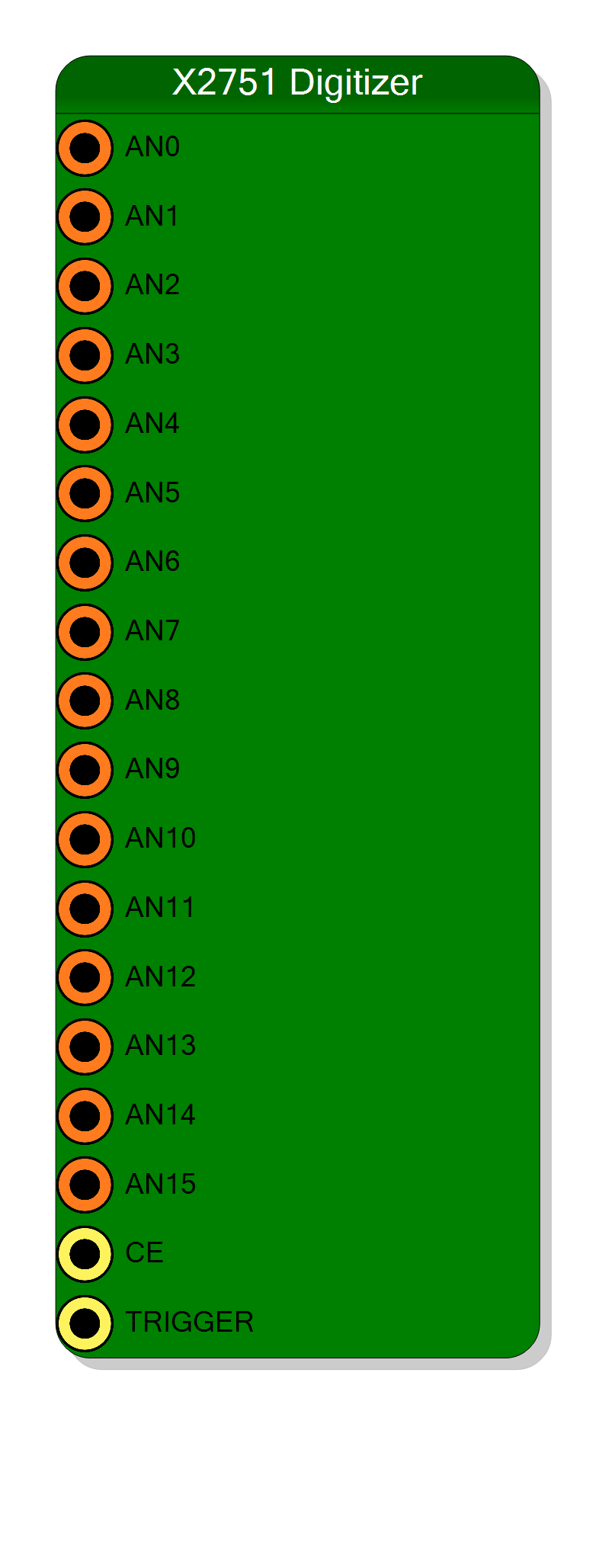
Waveform readout block for the X2751 board. Uses the high-speed DMA engine and DDR4 memory to capture and transfer time-multiplexed waveforms to the PC. All channels are acquired synchronously on trigger.
Introduction
The X2751 Digitizer block implements waveform readout using the high-speed DMA engine and the large DDR4 memory buffer inside the board. This block takes time-multiplexed (TM) signal vectors and, upon trigger, acquires and transfers them to the PC.
All acquisition parameters are configured by software using CAEN FELib or the SciCompiler-generated SDK. The acquisition is initialized by a LOW → HIGH transition of the TRIGGER input (except when software trigger is selected).
Important: The acquisition of all 16 channels is always synchronous - when the trigger fires, all channels are captured at the same instant.
Time multiplexing: the board has 16 channels sampling at 1 GS/s, and that is exactly why every ANx input is a time-multiplexed 16-bit port with a TM factor of 8 - it carries 8 samples = 128 bits per clock cycle.
At a glance:
| Channels | 16 |
| Sampling rate per channel | 1 GS/s |
| TM factor | 8 (eight samples per clock) |
| Bits per clock per channel | 128 |
| Symbol pins | AN0-AN15, CE, TRIGGER |
| Properties | none |
Pin Description
Channel Enable for per-sample decimation.
- HIGH: Current 128-bit word is captured
- LOW: Current 128-bit word is discarded
- Unconnected: All samples captured (forced to ‘1’)
Useful for reducing data rate or conditional sampling.
Acquisition trigger input. A LOW → HIGH transition starts the waveform readout process.
Important: The acquisition of all 16 channels is always synchronous. When trigger fires, all channels are captured at the same instant.
If software trigger is enabled via CAEN FELib, this pin can be left unconnected: it defaults to ‘0’.
Time-multiplexed waveform input channels (16 pads, one per board channel). Each pad carries 8 time-multiplexed 16-bit samples per clock, i.e. 128 bits per clock cycle (TM factor 8) - the 1 GS/s sampling rate of one channel.
Connect to ADC outputs or processing chain outputs. Unconnected channels are automatically forced to 0.
Properties
Usage
What the Digitizer Does
The Digitizer is NOT the ADC itself - it is the readout block that:
- Receives time-multiplexed waveform data from the analog inputs or processing chains
- Captures all 16 channels simultaneously when triggered
- Stores the waveforms in the DDR4 memory buffer
- Transfers the data to the PC via high-speed DMA
┌─────────────────────────────────────────────────────────────────┐
│ Digitizer Flow │
│ │
│ TM Signals ──►┌──────────────┐ ┌─────────┐ ┌─────┐ │
│ (16 ch, │ │ │ │ │ │ │
│ 128 bit/clk) │ DIGITIZER │════►│ DDR4 │════►│ DMA │═══╋══► PC
│ ══════════════│ │ │ Buffer │ │ │ │
│ TRIGGER ─────►│ │ │ │ │ │ │
│ └──────────────┘ └─────────┘ └─────┘ │
│ ▲ │
│ │ │
│ L→H starts acquisition │
└─────────────────────────────────────────────────────────────────┘
Synchronous Acquisition
All 16 channels are acquired synchronously. When the TRIGGER signal transitions from LOW to HIGH:
- All channel inputs are sampled at the same clock edge
- The acquisition continues for the configured record length
- Data is buffered in DDR4 for transfer to PC
This ensures perfect time alignment between channels for multi-channel analysis.
Time-Multiplexed Inputs
Each 16-bit ANx pin carries 8 consecutive samples per clock cycle - that is how a 1 GS/s channel fits into the design clock:
X2751 (TM Factor = 8):
┌─────────────────────────────────────────────────────────────────────────────┐
│ Clock Cycle N │
├─────────┬─────────┬─────────┬─────────┬─────────┬─────────┬─────────┬─────────┤
│ Samp 0 │ Samp 1 │ Samp 2 │ Samp 3 │ Samp 4 │ Samp 5 │ Samp 6 │ Samp 7 │
│ (16-bit)│ (16-bit)│ (16-bit)│ (16-bit)│ (16-bit)│ (16-bit)│ (16-bit)│ (16-bit)│
└─────────┴─────────┴─────────┴─────────┴─────────┴─────────┴─────────┴─────────┘
Total: 128 bits per clock per channel
Every block you connect upstream of the Digitizer must therefore be a TM block with the same TM factor. Connecting a plain 16-bit signal to an ANx pin is a size mismatch, not a decimation.
Typical Usage
Connect the Digitizer to receive waveforms from the analog inputs or processing chain outputs:
┌──────────────┐ ┌──────────────┐
│ Board │ │ X2751 │
│ Analog │ (or processing) │ Digitizer │
│ Inputs │ │ │
├──────────────┤ ├──────────────┤
│ AN_0 ────────┼────────────────────────►│ AN0 │
│ AN_1 ────────┼────────────────────────►│ AN1 │
│ ... │ │ ... │
│ AN_15 ───────┼────────────────────────►│ AN15 │
│ │ │ │
│ │ Trigger logic ──────►│ TRIGGER │
└──────────────┘ └──────────────┘
The block draws 16 ANx pads (AN0-AN15), one per board channel. Pads left unconnected are forced to 0.
Channel Enable (CE) Pin
The CE (Channel Enable) pin allows per-sample data decimation:
| CE State | Behavior |
|---|---|
| HIGH | Sample is captured and stored |
| LOW | Sample is discarded |
| Unconnected | All samples captured (CE forced to ‘1’) |
Use cases for CE:
- Reduce data rate by decimating samples
- Conditional sampling based on external logic
- Synchronize with external timing signals
CE gates the whole 128-bit word, not a single sample inside it: one CE pulse accepts or drops all 8 samples of that clock cycle.
Best Practices
- All channels synchronous: Remember that trigger affects all 16 channels simultaneously
- Unconnected channels: Channels without connections are forced to 0
- Trigger timing: Ensure trigger arrives when signals are stable
- CE usage: Use CE for decimation only when needed
- Buffer management: Monitor DDR4 buffer to avoid overflow
Resources & Timing
-
Latency: 1 clock cycle for trigger detection
-
Throughput: 16 channels × 8 samples per clock
- X2751: 16 × 8 = 128 samples per clock cycle (2048 bits)
- 16 channels at 1 GS/s, time-multiplexed by 8 onto 16-bit ports
- Data is buffered in DDR4 before DMA transfer to PC
- All channels acquired synchronously on trigger edge
Supported Boards
- X2751