CFD - TM (Constant Fraction Discriminator)
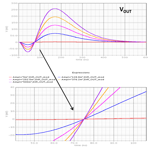
CFD_TM implements a Time-Multiplexed Constant Fraction Discriminator for precise timing measurements independent of pulse amplitude. By subtracting a scaled version of the input from a delayed copy, the zero-crossing point is tied purely to the pulse shape, eliminating timing walk errors. Supports optional sub-sample interpolation for picosecond-level timing resolution.
Introduction
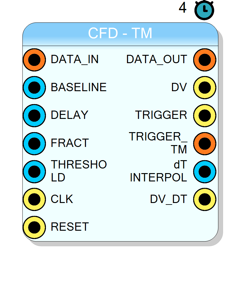
CFD_TM implements a Constant Fraction Discriminator optimized for time-multiplexed (TM) high-speed digitizer boards.
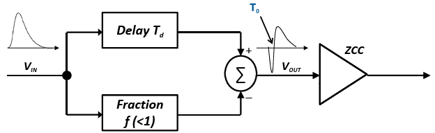
The CFD generates a precise timing marker by computing:
$$ V_{\mathrm{out}}(t) = V_{\mathrm{in}}(t - T_d) - f \cdot V_{\mathrm{in}}(t) $$
where:
- $T_d$ = programmable delay (in sample units)
- $f$ = constant fraction (0 < $f$ < 1)
Why CFD Eliminates Amplitude Dependence
If the input pulse is a scaled version of some shape $s(t)$ with amplitude $A$:
$$ V_{\mathrm{in}}(t) = A \cdot s(t) $$
Then:
$$ V_{\mathrm{out}}(t) = A \cdot [s(t - T_d) - f \cdot s(t)] $$
The zero-crossing condition $V_{\mathrm{out}}(t_{zc}) = 0$ becomes:
$$ s(t_{zc} - T_d) - f \cdot s(t_{zc}) = 0 $$
The amplitude $A$ cancels out! The timing depends only on the pulse shape and the CFD parameters, not on the signal amplitude.
Pin Description
ap_fixed<16,5> (5 integer bits, 11 fractional bits).
Add this to TRIGGER_TM index for precise timing.
Resolution: ~0.0005 samples (~1 ps @ 500 MS/s).
Properties
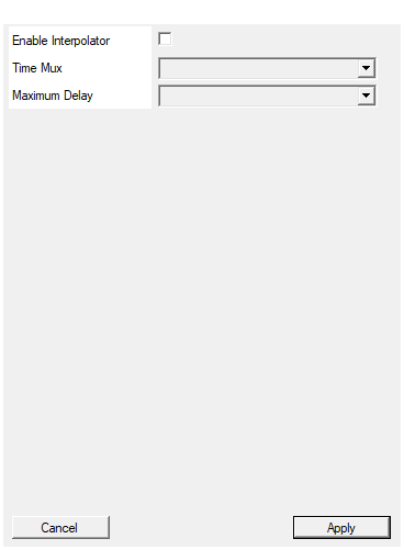
Default: False
Set number of samples for each clock cycle
Number of samples packed per clock word. Options: 2, 4, 8, 16, 32. Must match the input signal’s TM factor.Default: 4
Options: 2 4 8 16 32
Set delay memory element. Each memory element store a full TM word, so for example, with TM=4 each cell store 4 signal samples
Depth of the circular delay buffer (in TM words). Determines the maximum configurable delay. Options: 64, 128, 256, 512, 1024, 2048, 4096, 8192, 16384. Larger values use more BRAM resources.Default: 512
Options: 64 128 256 512 1024 2048 4096 8192 16384
Usage
Functional Overview
The CFD-TM block processes time-multiplexed data streams where multiple samples are packed into each clock word.
| Block | Function |
|---|---|
| Delay $T_d$ | Circular buffer holding delayed samples |
| Fraction $f$ | Scales the live input |
| Summer | Computes $V_{\mathrm{out}} = V_{\mathrm{delayed}} - f \cdot V_{\mathrm{live}}$ |
| Zero-Crossing Detector | Latches first crossing after arming |
| Interpolator | (Optional) Computes sub-sample position |
Operation
- Arming: The discriminator is armed when $V_{\mathrm{out}} < -\text{Threshold}$
- Triggering: Once armed, trigger fires on first $V_{\mathrm{out}} \geq 0$
- Output: TRIGGER pulse indicates event, dT_INTERPOLED provides fine timing
Timing Diagram
Time Multiplexing
The TM (Time Multiplexing) factor determines how many samples are packed per clock word:
| TM Factor | Samples/Word | Example Board |
|---|---|---|
| 2 | 2 × 16-bit | - |
| 4 | 4 × 16-bit | 500 MS/s @ 125 MHz CLK |
| 8 | 8 × 16-bit | 1 GS/s @ 125 MHz CLK |
| 16 | 16 × 16-bit | - |
| 32 | 32 × 16-bit | - |
Interpolation
When Enable Interpolator is selected, the block computes the precise sub-sample position of the zero-crossing using linear interpolation:
$$ x = \frac{-V_{\mathrm{out}}[n-1]}{V_{\mathrm{out}}[n] - V_{\mathrm{out}}[n-1]} $$
The dT_INTERPOLED output is a signed 16-bit fixed-point number:
| Field | Bits | Description |
|---|---|---|
| Sign | [15] | Sign bit |
| Integer | [14:11] | 4 bits magnitude → range: -16 to +15 |
| Fraction | [10:0] | 11 bits → resolution: $2^{-11} \approx 0.000488$ samples |
With 500 MS/s sampling (2 ns/sample), this gives ~1 ps timing resolution!
Latency
| Configuration | Latency |
|---|---|
| Without interpolation | 4 clock cycles |
| With interpolation | 54 clock cycles |
Note: When using TRIGGER for system timing, the input signal should be delayed by the same amount to maintain alignment.
Usage Tips
- Set DELAY to align $T_d$ with the desired pulse fraction (typically on the rising edge). Minimum value: 4 samples.
- Choose FRACT (e.g., 0.3-0.5) to optimize timing accuracy vs. noise. Value 0x0000 = 0, 0xFFFF = 1.
- Adjust THRESHOLD to avoid false triggers on noise but still catch real pulses.
- Use dT_INTERPOLED for sub-sample timing resolution.