
Right Shift [TM]
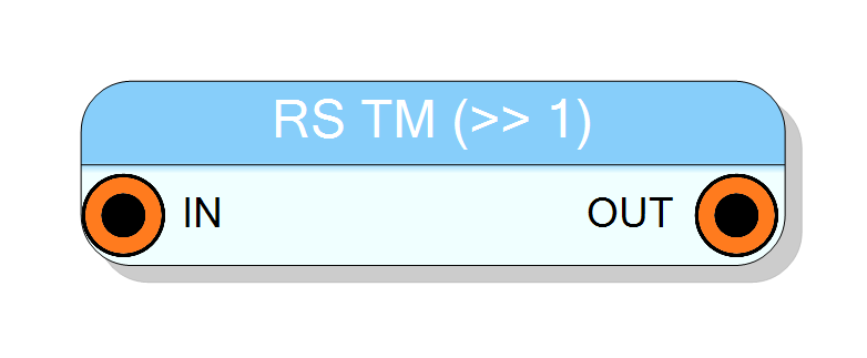
Time-multiplexed bitwise logical right shift operation. Shifts all bits of the input binary number to the right by a configurable amount, filling vacant leftmost positions with zeros. Does not preserve sign. Supports configurable output width and TM factors from 2 to 32. Pure combinational logic (zero latency).
Introduction
This block performs a logical right shift operation on time-multiplexed (TM) data streams. Each bit of the input is shifted right by the specified Shift amount, and zeros are inserted in the vacant leftmost positions.
The operation is purely combinational with zero clock latency:
$$ \mathrm{OUT}(n) = \mathrm{IN}(n) \gg S, $$
where $S$ is the Shift parameter. The TM Factor property determines how many parallel samples are processed per clock cycle.
Unlike arithmetic right shift, this logical shift does not preserve the sign bit (MSB). All vacant positions are filled with zeros regardless of the input’s MSB value.
Pin Description
Input Size × TM Factor
Each TM phase receives its corresponding slice of the input bus.
Logical right-shifted output, always TM (same factor as IN).
Width: Output Size × TM Factor
- Output Size = Input Size (SAME SIZE mode)
- Output Size = Input Size - Shift (SHIFTED SIZE mode)
Output is combinational (zero latency).
Properties
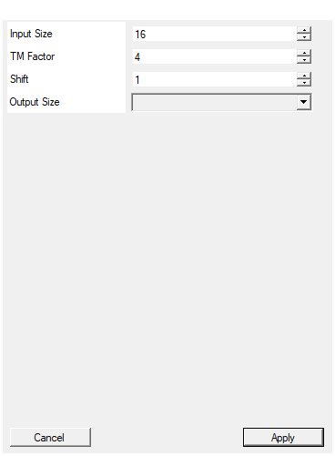
Set the input word size in bits (per phase)
Number of bits per input sample ($N_\text{in}$). Range: 2 – 16384. Each TM phase processes samples of this width.Default: 16
Range: 2 – 16384
Time Multiplexing factor (number of phases)
Time-multiplexing factor (number of parallel phases). Allowed values: 2, 4, 8, 16, 32 (up to 32). Higher values increase throughput proportionally but consume more FPGA resources (one shift instance per TM phase).Default: 4
Range: 2 – 32
Number of bit to be shifted
Number of bit positions to shift right ($S$). Range: 0 – 16384. When Shift = 0, output equals input (no operation). When Shift ≥ Input Size, output is all zeros.Default: 1
Range: 0 – 16384
Select if output should have same size of input or should be INPUT_SIZE-SHIFT
Output bit width mode:
SAME SIZE→ Output width = Input width (standard mode)SHIFTED SIZE→ Output width = Input width - Shift (truncated to remaining bits)
Choose SAME SIZE for standard shift operations. Choose SHIFTED SIZE when only the remaining bits are needed (reduced width).
Default: SAME SIZE
Options: SAME SIZE SHIFTED SIZE
Functional description
The component implements a bitwise logical right shift in VHDL, replicated N times (where N = TM Factor) to support time-multiplexed data streams.
For each TM phase, the operation is:
$$ y[i] = x[i] \gg S, $$
where:
- $x[i]$ → input sample at phase $i$
- $y[i]$ → output sample at phase $i$
- $S$ → shift amount (constant across all phases)
The logical right shift operation removes $S$ bits from the left and prepends $S$ zero bits:
$$ y = \lfloor x / 2^S \rfloor $$
Output size modes
The block offers two output width configurations:
-
SAME SIZE: Output width = Input width The output is the same size as input; shifted bits are preserved.
-
SHIFTED SIZE: Output width = Input width - Shift amount Only the remaining bits after the shift are output (truncated to smaller width).
Example
Given an 8-bit input 10110011 and shift amount = 3:
- Logical shift result:
00010110(3 MSBs discarded, 3 zeros prepended) - SAME SIZE (8 bits):
00010110 - SHIFTED SIZE (5 bits):
10110(only remaining bits)
Comparison with arithmetic shift
- Logical right shift: Always fills with zeros (unsigned division by 2^S)
- Arithmetic right shift: Fills with sign bit (signed division by 2^S)
Example with negative 8-bit number 11010110 (-42 in two’s complement), shift = 2:
- Logical:
00110101(53 unsigned) - Arithmetic:
11110101(-11, preserves sign)
Mathematical background
Logical right shift by $S$ positions is equivalent to unsigned integer division by $2^S$:
$$ x \gg S = \lfloor x / 2^S \rfloor $$
This is commonly used for:
- Fast unsigned division by powers of 2
- Bit extraction and manipulation
- Scaling in fixed-point arithmetic (unsigned values)
- Unpacking bit fields
Timing
The component is purely combinational with zero latency:
| Property | Latency (clock cycles) |
|---|---|
| Right Shift TM | 0 |
All TM phases are processed in parallel within the same clock cycle.
Typical use cases
- Fast unsigned division by powers of 2 in signal processing
- Bit field extraction and unpacking
- Fixed-point rescaling (unsigned values)
- Building blocks for barrel shifters and ALUs
- Converting between different unsigned fixed-point formats
Waveform example
Example with TM Factor = 4, Shift = 2, Input = [0xC, 0xF, 0xA, 0x7] (4-bit), SAME SIZE mode.
Note: Output is available immediately (combinational logic). Values shown in hex: 0xC » 2 = 0x3, 0xF » 2 = 0x3, 0xA » 2 = 0x2, 0x7 » 2 = 0x1.