
List ESS
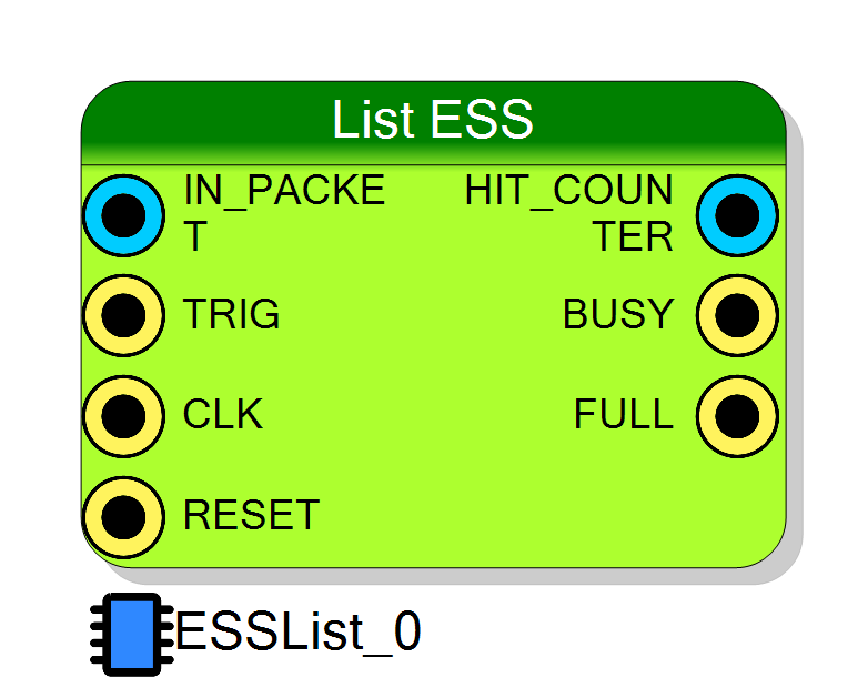
Event list block for the ESS (European Spallation Source) FEA framework. On every TRIG edge it latches a fixed-size event made of N 32-bit words and pushes it, as one AXI-Stream frame terminated by TLAST, into the board’s bulk-data link towards the ESS back-end. There is no PC read-out FIFO: the data leaves the board over the ESS optical link, not over SciSDK.
Introduction
Principle of Operation
The List ESS block is the list-mode front end of the ESS FEA framework
(the firmware bundle used for detectors at the European Spallation Source).
It is a fixed-length event recorder: every accepted trigger produces exactly
WordCount 32-bit words, taken in one shot from the IN_PACKET bus.
What makes it “ESS”
The standard List block ends in a read-out FIFO that the PC drains through
the register bus (BUS_<endpoint>_READ_DATA), and SciSDK reads it as a
ListModule. The List ESS block ends somewhere completely different: its
output is an AXI-Stream master wired to the board’s bulk data port
(bkdata_s_axis_*), which in the ESS top level goes into the fea_top core
and out over the gigabit transceivers to the ESS back-end.
| List | List ESS | |
|---|---|---|
| Where the data goes | PC, over the register/USB/Ethernet bus | ESS back-end, over the FEA bulk-data link |
| Read-out interface | FIFO read port + STATUS register |
32-bit AXI-Stream with TLAST |
| Event framing | none — a raw word stream | one TLAST-terminated frame per event |
| Software registers | STATUS (R) + CONFIG (W) |
CONFIG (W) only |
| Event size | 1 word of Wordsize bits |
WordCount x 32 bits |
| Event counter | not exposed | HIT_COUNTER output pin |
| Read out with SciSDK | yes | no — nothing to read |
Because the FPGA-side read-out is gone, the only thing software can do with this
block is start, stop, reset and flush it through one CONFIG register. Everything
else — where the events end up, how they are packed into UDP/ESS frames, how they
are timestamped downstream — is the job of the ESS FEA framework, not of this block.
Pin Description
Event payload – the whole event, presented in parallel.
Word i of the transmitted frame is IN_PACKET(32*i+31 downto 32*i),
so bits [31:0] are sent first and the most significant slice last.
Sampled on the second clock edge after TRIG rises; it must still be
valid at that moment.
Event trigger – a rising edge requests one event.
Double-registered internally, so the capture happens two clock edges later.
The request is dropped if CONFIG[0] = 0 or if an overflow flag is set.
Level-holding this pin high yields one event, not a burst.
HIT_COUNTER and forces BUSY high.
Defaults to the project global reset when left unconnected.
Accepted-event counter – free-running 32-bit count of the triggers this
block has actually accepted (not of the triggers presented). It wraps at
2³² and is cleared by RESET or by CONFIG[1].
Comparing it against your own trigger count is the cheapest way to detect that events are being dropped.
Stopped indicator – BUSY = NOT CONFIG[0].
It is high while the block is stopped (and during reset) and low while it is
running. Note that, unlike the standard List block, it does not go high on
a full buffer — watch FULL for that.
overflow, i.e. a write has just been lost. It is an after-the-fact,
short-lived indication, not a back-pressure signal.
Properties
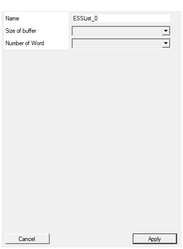
Set the name of the endpoint
Name of the memory-mapped endpoint. It is what the CONFIG register is named
after in the register map (REG_<EndpointName>_CONFIG_WR) and what identifies
the block in RegisterFile.json.
Must be unique in the design.
Default: ESSList_0
Default: ESSList_0
Size of the readout buffer. Buffer must be large enought to compensate readout bus stalls.
Depth of each per-word FIFO, in events, and also the depth of the
cross-domain FIFO (in words). It maps to the memLength generic.
Available values: 128, 256, 512, 1024, 2048, 4096, 8192, 16384, 32768, 65536.
This is the burst tolerance of the block: it is how many events can arrive
faster than the ESS link drains them before writes start being lost. Larger
values cost WordCount more block-RAM lanes.
Default: 1024
Default: 1024
Options: 128 256 512 1024 2048 4096 8192 16384 32768 65536
Set the number of 32 bits words
Number of 32-bit words in one event — that is, the size of the IN_PACKET
pin (WordCount x 32 bits) and the number of AXI-Stream beats in the frame
sent for each trigger. Maps to the G_NUM_WORDS generic.
Available values: 1 … 32.
Changing it rebuilds the symbol (the IN_PACKET pin changes width) and costs
one 32-bit FIFO lane per word. It also sets the drain cost per event
(WordCount + 2 clocks).
Note that the value published in RegisterFile.json is fixed at 4 words and
does not follow this property.
Default: 4
Default: 4
Options: 1 2 3 4 5 6 7 8 9 10 11 12 13 14 15 16 17 18 19 20 21 22 23 24 25 26 27 28 29 30 31 32
⚙️ Detailed Operation
Data flow
CLK (acquisition domain) BUS_CLK (bulk-data domain)
┌───────────────────────────────────────────┐ ┌────────────────────────────┐
│ │ │ │
│ IN_PACKET ──┬─[31:0]──► FIFO word 0 ──┐│ │ │
│ (N x 32) ├─[63:32]─► FIFO word 1 ──┤│ │ │
│ ├─ ... ─► ... ──┼┼─┼──► bkdata_s_axis_tdata[31:0]
│ └─[32N-1: ► FIFO word N-1─┘│ │ bkdata_s_axis_tvalid │
│ 32N-32] ▲ │ │ bkdata_s_axis_tlast │
│ │ │ │ ◄──bkdata_s_axis_tready │
│ TRIG ──► edge detect ───────┘ │ │ │
│ │ │ │ │
│ └──► HIT_COUNTER (32 bit) │ │ │
└───────────────────────────────────────────┘ └────────────────────────────┘
N per-word synchronous FIFOs one 33-bit async FIFO
(depth = BufferSize, XPM sync) (data[31:0] + last)
The block is built from two stages:
- Capture.
WordCountindependentxpm_fifo_syncbuffers, each 32 bits wide andBufferSizedeep, all written on the same write strobe. Word i of the event isIN_PACKET(32*i+31 downto 32*i), so the least significant 32 bits ofIN_PACKETare sent first. - Serialise + cross. A small FSM reads the N buffers one after the other and
writes a 33-bit
{data, last}token into anxpm_fifo_asyncthat crosses fromCLKtoBUS_CLK. The FIFO runs in FWFT mode, so its output is the AXI-Stream master:data_valid → TVALID,dout(32:1) → TDATA,dout(0) → TLAST, andTREADYdrives the read enable.
Trigger acceptance and sampling instant
TRIG is put through two registers before the edge is detected
(iTrig <= TRIG; oTrig <= iTrig; then iTrig='1' and oTrig='0'). The consequence
matters for the surrounding logic:
- The event is accepted on the second clock edge after
TRIGgoes high. IN_PACKETis sampled on that same edge — so the payload must still be valid two clock edges after theTRIGrising edge, not on the edge that raisesTRIG.- Because the detector is edge based, holding
TRIGhigh does not produce a stream of events: it produces exactly one.
A trigger is accepted only when all of these hold:
accept = rising_edge(TRIG) AND CONFIG[0] = 1 AND no per-word overflow flag set
Draining an event
Once the N per-word buffers hold an event, the FSM walks through them:
s_idle : wait for (buffer 0 not empty) and (async FIFO not prog_full)
s_read : one word per clock, word_index = 0 .. WordCount-1
on the last word: set TLAST, pop all N buffers
s_last : one turnaround clock
→ s_idle
So one event costs WordCount + 2 clock cycles on the acquisition clock to
move into the cross-domain FIFO. That is the sustained event-rate ceiling of the
block; the per-word buffers absorb bursts above it, up to BufferSize events.
The FSM also stalls while the async FIFO’s prog_full is asserted. That threshold
is set to BufferSize - 3 * WordCount, i.e. it always leaves room for three whole
events, so a frame is never cut in half by back pressure from the ESS link.
CONFIG register
This is the only register the block owns (write only).
| Bit | Function |
|---|---|
| 0 | Run. 0 holds the block stopped: triggers are ignored and BUSY is high. |
| 1 | Force reset. Clears HIT_COUNTER, asserts the FIFO reset, forces BUSY high. |
| 2 | FIFO flush. Level-sensitive: while it is 1 the FIFO reset is held asserted. |
There is no STATUS register — the memory-mapped component is declared as a
generic endpoint with a single CONFIG register, not as a list. Use the
HIT_COUNTER, BUSY and FULL pins in the design if you need visibility.
Overflow behaviour
Word order and byte order
Words are streamed exactly as they appear on IN_PACKET, least significant
32-bit slice first, with no byte swapping. (If you need the ESS on-the-wire
big-endian order, do it upstream of this block, or use Custom Packet ESS,
which has a Byte Swap option.)
Simulation
The compiler writes a different core when the project is simulated: it has no
CONFIG port and hardwires the configuration word to x"00000001", so the block
is permanently running. Everything else — the FIFOs, the FSM, the AXI-Stream
output — is identical. There is no file dump: to observe the data in a simulation,
probe bkdata_s_axis_* in the waveform viewer.
Compiler messages
| Message | Meaning |
|---|---|
Generating HDL code for <designator> |
normal, informational |
Generating memory mapped component: <endpoint> |
the CONFIG register is being placed |
SDK address undefined for <endpoint> |
error — the endpoint got no base address; the design cannot be built |
Software / SciSDK
There is no SciSDK read-out path for this block. CompileSDK emits a JSON
descriptor only, of type ListModuleESS, carrying the endpoint name, base
address and the CONFIG register. Software uses it to find CONFIG; the event
data never reaches SciSDK.
One bulk-data master per design
The AXI-Stream ports are connected directly to the top-level bkdata_s_axis_*
signals (the compiler does not create a signal, it binds to the existing one).
There is no arbiter between several producers, so a design must contain exactly
one block driving the bulk-data stream — one List ESS or one Custom Packet ESS,
not two of either and not one of each.
Quick reference
| Item | Value |
|---|---|
| Event size | WordCount x 32 bits (1 … 32 words) |
| Buffer | BufferSize events per word lane |
| Output | 32-bit AXI-Stream, one TLAST frame per event |
| Output clock | BUS_CLK (bulk-data domain) |
| Drain cost | WordCount + 2 acquisition clocks per event |
| Registers | CONFIG (write) only |
| Boards | R5560-B / DAQ14125-B with FPGA model Z-7035-ESS |
Resources & Timing
- Throughput: One event per WordCount + 2 acquisition clock cycles, sustained
WordCountsynchronous 32-bit FIFOs ofBufferSizeentries, plus one 33-bit asynchronous FIFO ofBufferSizeentries (all XPM, block RAM).- The only clock-domain crossing is the async FIFO between
CLKandBUS_CLK. - No multipliers, no DSP.
- Requires the ESS FEA framework: the board must be an R5560-B / DAQ14125-B
with FPGA model
Z-7035-ESS, and the framework path must be configured inboards/<board>_dll/ess.txt, otherwise the compiler stops with “You need to specify the ESS FEA framework path … to use the ESS FEA framework.”