
Gate Differentiator (TM)
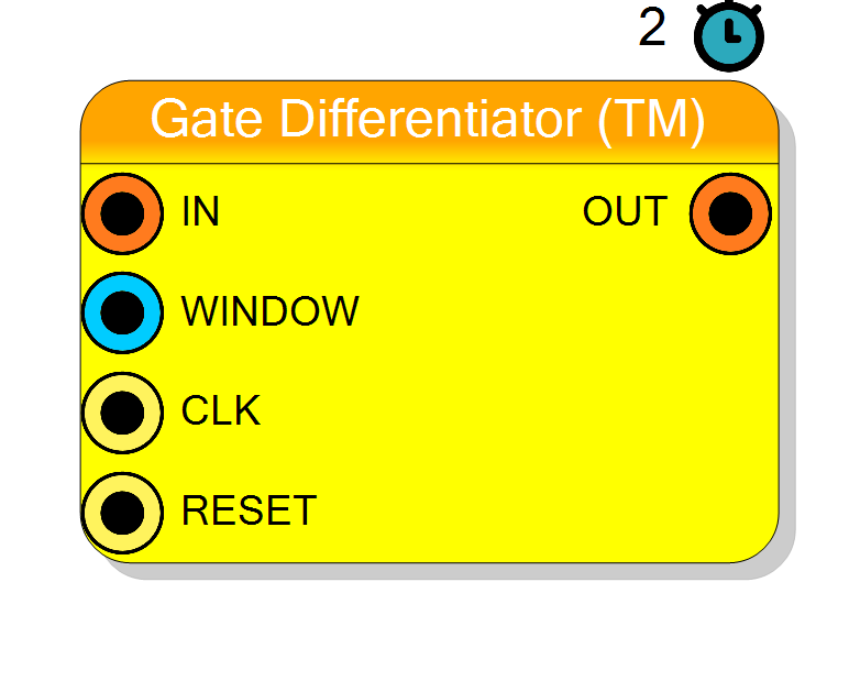
Time-multiplexed programmable differentiator with configurable delay window. Computes the difference between current sample and a delayed sample stored in BRAM circular buffer. Window size is runtime programmable (1 to 1024 samples per TM lane). Output is always signed with width = input width + 1 bit. Latency: 2 clock cycles.
Introduction
This block computes the programmable-window difference for each TM phase
independently. Each TM lane maintains its own BRAM-based delay line, and the
output is the difference between the current input and a sample from WINDOW
cycles ago.
On every rising edge of CLK, for each TM phase $i$:
$$ \mathrm{OUT}_i[n] = \mathrm{IN}_i[n] - \mathrm{IN}_i[n - W], $$
where $W$ is the programmable window size (runtime configurable via WINDOW input).
The output is always signed with width = Input bits + 1 to prevent overflow.
Pin Description
Input bits × TM Factor
Each TM lane has an independent circular buffer for delay.
Delay window size, scalar (not TM), runtime programmable. Width: $\lceil \log_2(\text{Window Max} + 1) \rceil$ bits Valid range: 1 to Window Max. Applied to all TM lanes simultaneously.
Example: Window Max = 1024 → WINDOW width = 11 bits, range [1, 1024]
(Input bits + 1) × TM Factor
Each TM lane contains $\text{IN}[n] - \text{IN}[n - \text{WINDOW}]$.
Valid after 2 clock cycles + WINDOW sample delay.
Properties
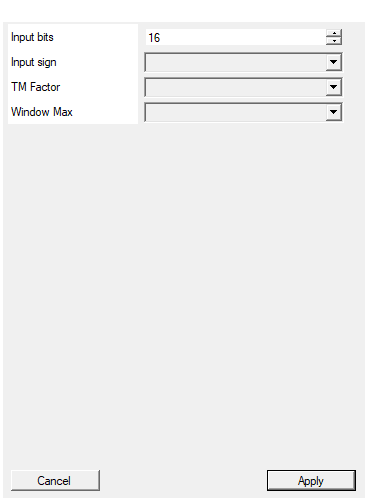
Set the number of bits of the input per sample
Number of bits per input sample ($N_\text{in}$). Range: 4 – 32. Output width is automatically set to $N_\text{in} + 1$.Default: 16
Range: 4 – 32
Select the sign/unsign of the input
Input arithmetic type:
- UNSIGNED → Non-negative integers [0, $2^{N}-1$]
- SIGNED → Two’s complement [$-2^{N-1}$, $2^{N-1}-1$]
Note: Output is always SIGNED regardless of input sign, with width = Input bits + 1.
Default: UNSIGNED
Options: UNSIGNED SIGNED
Select the Time Multiplexing factor (samples per word)
Number of time-multiplexed phases (parallel differentiators). Allowed values: 2, 4, 8, 16, 32.
Each TM lane has an independent circular buffer of depth = Window Max.
Default: 4
Options: 2 4 8 16 32
Maximum window size for programmable differentiation (in sample phases). Stored in BRAM.
Maximum delay window size (buffer depth per TM lane), stored in BRAM. Allowed values: 64, 128, 256, 512, 1024.
Larger buffers consume more BRAM:
- BRAM usage ≈ (Input bits) × (Window Max) × (TM Factor) / 18432 blocks
The WINDOW input can dynamically select any delay from 1 to Window Max
at runtime without reconfiguration.
Default: 64
Options: 64 128 256 512 1024
Functional description
The component implements N independent programmable differentiators using Xilinx HLS, with each TM lane having its own BRAM-based circular buffer for sample storage.
Operation
For each TM phase $i \in [0, N-1]$:
$$ y_i[n] = x_i[n] - x_i[n - W], \qquad W \in [1, \text{WindowMax}] $$
where:
- $x_i[n]$ →
IN(TM phase $i$) - $y_i[n]$ →
OUT(TM phase $i$, signed) - $W$ →
WINDOW(runtime programmable, applied to all TM lanes) - $N$ → TM Factor
Delay buffer
Each TM lane maintains:
- Circular buffer of depth = Window Max (stored in BRAM)
- Write pointer that auto-increments each clock cycle
- Read pointer = write pointer -
WINDOW
The delayed sample $x[n-W]$ is fetched from BRAM using the read pointer.
Output characteristics
- Sign: Always SIGNED (two’s complement), regardless of input sign
- Width: Input bits + 1 (prevents overflow from subtraction)
- Range: $[-2^{N_\text{in}}, +2^{N_\text{in}}]$ for unsigned input, $[-2^{N_\text{in}}, +2^{N_\text{in}}-1]$ for signed input
Example: 16-bit unsigned input → 17-bit signed output, range [-65536, +65536]
Mathematical background
For window size $W$, the discrete-time transfer function is:
$$ H_i(z) = 1 - z^{-W} $$
This is a finite impulse response (FIR) highpass filter with:
- Zeros at $z = e^{j2\pi k / W}$ for $k = 0, 1, \ldots, W-1$
- Null at DC ($\omega = 0$), ideal for removing baseline
- Linear phase (symmetric impulse response)
- Peak gain of 2 at Nyquist frequency (for small $W$)
The programmable window allows runtime adjustment of:
- Highpass cutoff frequency: $f_c \approx f_s / (2\pi W)$
- Sensitivity to rate of change: larger $W$ → smoother derivative
Comparison with fixed differentiator
| Component | Window | Output Width | Use Case |
|---|---|---|---|
| Differentiator (TM) | Fixed 1 | Input bits + 1 | Simple backward difference |
| Differentiator Programmable | 1-1024 | Input bits + 1 | Configurable baseline removal |
Timing
The HLS-generated IP has a fixed latency of 2 clock cycles:
| Property | Latency (clock cycles) |
|---|---|
| Gate Differentiator (TM) | 2 |
Total system delay: T_delay = 2 × T_CLK.
Note: This does not include the group delay of $W/2$ samples introduced by the differencing window itself.
BRAM usage
Each TM lane requires a circular buffer:
$$ \text{BRAM per lane} = \frac{\text{Input bits} \times \text{Window Max}}{18432} $$
Total BRAM usage: $$ \text{Total BRAM} = \text{TM Factor} \times \text{BRAM per lane} $$
Example: 16-bit input, TM=8, WindowMax=1024 → $\frac{16 \times 1024}{18432} \times 8 \approx 7.1$ BRAM blocks
Typical use cases
- Baseline removal with programmable window in spectroscopy
- Pulse detection with adjustable derivative scale
- Edge detection in multi-channel ADC data
- Programmable highpass filtering
- Time-domain feature extraction (slope, peaks)
Waveform example
Example with TM Factor = 4, WINDOW = 2, Input = [10, 20, 30, 40, 50, …].
Note: OUT[n] = IN[n] - IN[n-2], e.g., 50-10=40, 60-20=40, etc., with 2 cycle latency.