
Multichannel Register (CH-Register)
Creates multiple identical registers with sequential addresses for multi-channel configurations. Ideal when the same parameter needs different values for each channel.
Introduction
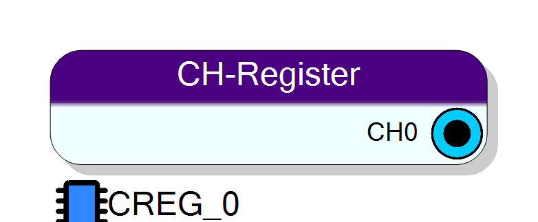
The Multichannel Register (CH-Register) block creates multiple identical registers with a single component, where each register controls a different channel. This is the ideal solution when you need the same parameter (e.g., threshold, gain, offset) applied to many channels with different values.
Key difference from Register File:
- Register File: Many different parameters (threshold, gain, enable, mode…)
- CH-Register: Same parameter for many channels (threshold_0, threshold_1, threshold_2…)
Pin Description
Channel output/input pin (x = 0 to N-1).
- OUT direction: Outputs the register value to FPGA logic
- IN direction: Captures FPGA signal for software readback All channels have identical bit width set by Bits property. CH0 is the first of the family: the block declares CH0 .. CH(N-1), one per Number of Channels, and they are identical apart from their index. Each maps to one register slot of the endpoint: an OUT channel is driven from the host write register and mirrored back for read-back, an IN channel is captured for the host to read.
Properties
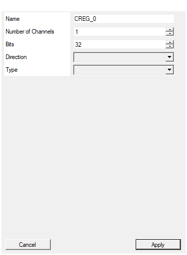
Set the name of the endpoint
Default: CREG_0
Define the number of channels
Number of channel registers to create. Each channel gets its own output/input pin and sequential address. Range: 1 to 1024, default 1.Default: 1
Define the number of bits
Default: 32
Define direction of registers
Direction of all channel registers.
- OUT: Software writes → FPGA outputs (configuration)
- IN: FPGA inputs → Software reads (status/readback) Default: OUT.
Default: OUT
Options: OUT IN
Define signal type
Data type for all channel registers.
- BIT VECTOR: std_logic_vector with specified bit width
- INTEGER: 32-bit integer type Default: BIT VECTOR.
Default: BIT VECTOR
Options: BIT VECTOR INTEGER
"THRESHOLD" generates SCI_REG_THRESHOLD_CH0, SCI_REG_THRESHOLD_CH1, etc.
Default: CREG_0.
Usage
When to Use Multichannel Register
Use the CH-Register when you need:
- Per-channel parameters: Same configuration applied to multiple channels
- Array-like access: Sequential addresses for easy iteration
- Uniform structure: All registers have identical size and type
- Scalable design: Easy to change channel count without redrawing
CH-Register vs Register File
| Feature | CH-Register | Register File |
|---|---|---|
| Registers | All identical | Each can be different |
| Names | CH0, CH1, CH2… | Custom names |
| Use case | Same param, many channels | Many different params |
| Configuration | Properties only | Graphical editor |
| Typical count | 4-1024 channels | 2-20 registers |
Example comparison:
CH-Register "THRESHOLDS" (8 channels): Register File "CONFIG":
├── CH0 (16-bit OUT) ├── THRESHOLD (16-bit OUT)
├── CH1 (16-bit OUT) ├── GAIN (8-bit OUT)
├── CH2 (16-bit OUT) ├── OFFSET (16-bit OUT)
├── CH3 (16-bit OUT) ├── ENABLE (1-bit OUT)
├── CH4 (16-bit OUT) ├── MODE (2-bit OUT)
├── CH5 (16-bit OUT) └── STATUS (8-bit IN)
├── CH6 (16-bit OUT)
└── CH7 (16-bit OUT)
Memory Mapping
CH-Register creates registers with sequential addresses, perfect for array-style access:
Base Address: 0x2000 (assigned by compiler)
CH-Register "THRESHOLDS" (8 channels, 16-bit):
┌─────────────┬──────────┬─────────┐
│ Channel │ Offset │ Address │
├─────────────┼──────────┼─────────┤
│ CH0 │ +0 │ 0x2000 │
│ CH1 │ +1 │ 0x2001 │
│ CH2 │ +2 │ 0x2002 │
│ CH3 │ +3 │ 0x2003 │
│ CH4 │ +4 │ 0x2004 │
│ CH5 │ +5 │ 0x2005 │
│ CH6 │ +6 │ 0x2006 │
│ CH7 │ +7 │ 0x2007 │
└─────────────┴──────────┴─────────┘
This allows efficient loop-based programming:
c
// Set all thresholds using base address + offset
for (int ch = 0; ch < 8; ch++) {
REG_WRITE(SCI_REG_THRESHOLDS_CH0 + ch, threshold_values[ch]);
}
Direction: OUT vs IN
| Direction | Description | Use Case |
|---|---|---|
| OUT | Software writes → FPGA outputs | Per-channel configuration (thresholds, gains, enables) |
| IN | FPGA inputs → Software reads | Per-channel status (counts, flags, measurements) |
OUT mode (most common):
Software ──write──► Register ──output──► FPGA Logic
│
▼
(e.g., comparator threshold)
IN mode:
FPGA Logic ──input──► Register ──read──► Software
│
▼
(e.g., event counter per channel)
Practical Example: 16-Channel Discriminator
Scenario: Configure thresholds for 16 discriminator channels
CH-Register Configuration:
├── Name: "DISC_THRESHOLD"
├── Number of Channels: 16
├── Bits: 12
├── Direction: OUT
└── Type: BIT VECTOR
Resulting Symbol:
┌────────────────────────┐
│ CH-Register │
│ "DISC_THRESHOLD" │
├────────────────────────┤
│ ◄── CH0 [11:0] │───► Discriminator 0
│ ◄── CH1 [11:0] │───► Discriminator 1
│ ◄── CH2 [11:0] │───► Discriminator 2
│ ... │
│ ◄── CH15 [11:0] │───► Discriminator 15
└────────────────────────┘
This approach keeps:
- Global parameters in Register File (one value for all)
- Per-channel parameters in CH-Registers (different value per channel)
Best Practices
- Name by parameter: Use
"THRESHOLD"not"CREG_0"- channels are numbered automatically - Match channel count: Set to actual number of channels in your system
- Use loops in software: Take advantage of sequential addressing
- Consider INTEGER type: Simplifies software when values are numeric
- Group related parameters: One CH-Register per parameter type
Resources & Timing
-
Latency: 1 clock cycle (synchronous to bus clock)
-
Throughput: 1 register access per bus cycle
Registers are mapped to sequential addresses starting from base. No FPGA fabric resources - direct bus interface mapping.