
RF Mixer
Sample-by-sample complex multiplier used to translate a signal between two frequency bands. Each of the two inputs (A, B) can independently be a real or complex (I/Q) stream, and the output can independently be real or complex. The HLS core is fully pipelined at II=1.
Introduction
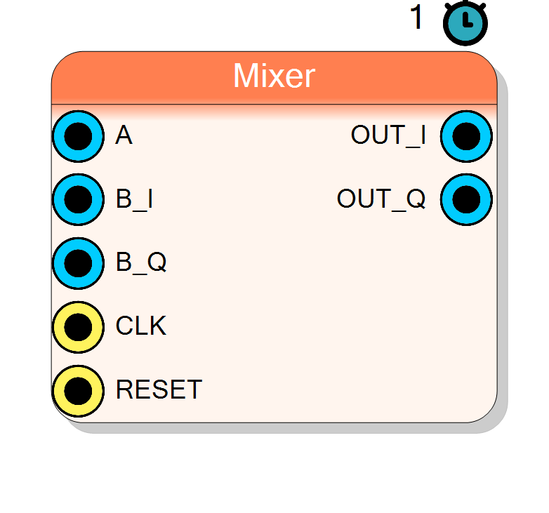
The Mixer block computes the product of two streams A and B on every clock cycle. In RF terms this is the classical “signal * local oscillator” operation used to translate a signal in the frequency domain (up/down-conversion, complex demodulation, tone shifting, …).
A ─────────┐
│
┌──▼──┐
│ X ├──► OUT
└──▲──┘
│
B ─────────┘
The three sides of the block can independently be real (single wire) or complex (I/Q pair). All eight combinations of A / B / OUT real-or-complex are supported. Behind the scene the block always computes the full complex product; when a side is declared real its imaginary component is forced to zero at synthesis time, so no extra hardware is generated.
Pin Description
ar = a, ai = 0.
Signed two’s complement, Input Bit Width bits.
ar*br - ai*bi, and the
default shape of this output. Present only when
Output is Complex = Complex. Signed; the width follows the
Output Width property: 2InputSize + 1 for M+N+1 (full),
2InputSize for M+N (sat), InputSize for max(M,N).
Properties
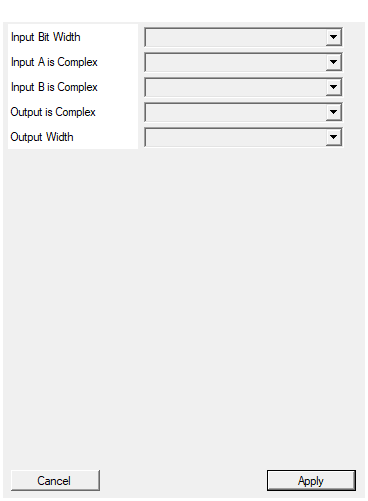
Bit width of the input samples (both A and B). Each I / Q component of a complex input uses this width.
Bit width of each I / Q component of both inputs. The output components are always2 * InputSize + 1 bits wide.
Range 4 to 32, default 16.
Default: 16
Options: 4 5 6 7 8 9 10 11 12 13 14 15 16 17 18 19 20 21 22 23 24 25 26 27 28 29 30 31 32
If TRUE the A input exposes I and Q pins. If FALSE a single A pin is used (Q is assumed zero).
Real / Complex topology of input A.
- Real (default) : single pin
A, imaginary part treated as 0. - Complex : two pins
A_IandA_Q.
Default: Real
Options: Real Complex
If TRUE the B input exposes I and Q pins. If FALSE a single B pin is used (Q is assumed zero).
Real / Complex topology of input B.
- Real : single pin
B, imaginary part treated as 0. - Complex (default) : two pins
B_IandB_Q.
Default: Complex
Options: Real Complex
If TRUE the OUT bus exposes I and Q pins. If FALSE only the real part (a_rb_r - a_ib_i) is exported.
Real / Complex topology of the output.
- Real : only
OUTpin, carriesa_r*b_r - a_i*b_i. - Complex (default) :
OUT_IandOUT_Qpins with the full complex product.
Default: Complex
Options: Real Complex
M+N+1 = full precision (no loss). M+N = drop the guard bit, SATURATE on the rare complex-product overflow. max(M,N) = shift right by min(M,N) then SATURATE to the input width (no growth). M=N=Input Bit Width here.
Default: M+N+1 (full)
Options: M+N+1 (full) M+N (sat) max(M N)
Usage
Mathematical model
Both inputs are seen as complex numbers A = a_r + j*a_i and
B = b_r + j*b_i. When a side is declared real its imaginary part is
zero.
The full complex product is:
OUT_r = a_r * b_r - a_i * b_i
OUT_i = a_r * b_i + a_i * b_r
The block always produces OUT_r. If the Output is Complex property
is on it also produces OUT_i, otherwise OUT_i is not routed out.
Bit widths
All four I / Q components of the two inputs share the same width, set by the Input Bit Width property. Data is treated as signed two’s complement.
The output components are always 2 * InputSize + 1 bits wide. This is
the full-precision result of the complex multiplication (worst case:
a_r*b_r - a_i*b_i with both terms saturated). The user is free to
truncate downstream if fewer bits are desired.
Pin topology depending on the properties
| A | B | OUT | Input pins | Output pins |
|---|---|---|---|---|
| Real | Real | Real | A, B | OUT |
| Real | Complex | Real | A, B_I, B_Q | OUT |
| Complex | Real | Real | A_I, A_Q, B | OUT |
| Complex | Complex | Real | A_I, A_Q, B_I, B_Q | OUT |
| Real | Real | Complex | A, B | OUT_I, OUT_Q |
| Real | Complex | Complex | A, B_I, B_Q | OUT_I, OUT_Q |
| Complex | Real | Complex | A_I, A_Q, B | OUT_I, OUT_Q |
| Complex | Complex | Complex | A_I, A_Q, B_I, B_Q | OUT_I, OUT_Q |
Changing any of the three is Complex properties re-designs the symbol because the pin set changes.
Typical applications
- Down-conversion: A = ADC baseband (real), B = numerically-controlled oscillator (complex), OUT = complex baseband.
- Up-conversion: A = complex baseband, B = NCO tone (complex), OUT = real if the RF DAC is real, complex if the DAC takes I/Q.
- Multiplier: real*real -> real product.
- Tone tagging in coherent detection.
Timing
The HLS core is compiled with #pragma HLS PIPELINE II=1, so it accepts
one new sample pair every clock cycle. The latency is 1 clock cycle
(result of cycle N is visible on OUT at cycle N+1). All ports use the
ap_none interface (plain combinational data, no ready/valid handshake).
Reset
The block exposes CLK and RESET inputs. RESET is the HLS synchronous
reset (ap_rst) as generated by Vitis HLS. The block has no internal
state that carries across samples, so the reset only clears the pipeline
registers to a known value.
Resources & Timing
-
Latency: 1 clock cycle
-
Throughput: 1 sample per clock (II=1)
Implemented with Vitis HLS. Each multiplier uses one DSP48 slice (or two for wider inputs). A complex-complex configuration uses four multipliers plus one adder and one subtractor. A real-real configuration uses one multiplier.